
Automotive GNSS Antenna PCB: Phase Center Stability Dominated by Lamination Symmetry and Copper Thickness Tolerance
1. The Millimeter That Decides the Meter
Autonomous driving, lane-level navigation, and precision agriculture all depend on real-time kinematic GNSS positioning with centimeter-level accuracy. The RTK algorithm itself is well understood — carrier-phase differential processing can resolve ambiguities and deliver ±1 cm horizontal accuracy under good conditions.
But the algorithm can only work with what the antenna delivers. And the antenna delivers a phase measurement that is referenced to a point in space called the phase center.
For a high-precision GNSS antenna, the phase center must remain stable across all satellite elevation and azimuth angles, across all frequency bands (L1, L2, L5, E1, E5a, B1, B2a), and across the full automotive temperature range (-40°C to +105°C). The industry benchmark is phase center variation of less than 0.5 mm for RTK-grade antennas; ordinary GPS antennas may exhibit 3–5 mm of phase center offset, which is sufficient for navigation but wholly inadequate for centimeter-level positioning.
The relationship between phase center stability and positioning accuracy is direct. Industry testing data shows that every 1 mm of additional phase center offset produces 0.1° of angular error at a 1,000-meter operating distance. For an autonomous vehicle approaching a junction at highway speed, 0.1° of angular error translates into decimeters of lateral position uncertainty — enough to matter.
The dominant contributors to phase center instability are not the antenna's radiating element design alone. They are manufacturing tolerances in the PCB: specifically, the symmetry of the lamination stack-up and the tolerance of the copper foil thickness. These two parameters determine whether the feed network's electrical length is identical on all four feed ports, and whether the ground plane remains flat and parallel to the radiating patch across temperature and mechanical stress.
This article examines the physical mechanisms by which lamination asymmetry and copper thickness tolerance dominate phase center stability in automotive GNSS antenna PCBs, quantifies the impact of each, and provides design and manufacturing guidelines for achieving sub-0.5 mm phase center variation in production.
2. The GNSS Antenna PCB: Architecture and Phase Center Physics
2.1 The Multi-Feed Patch Architecture
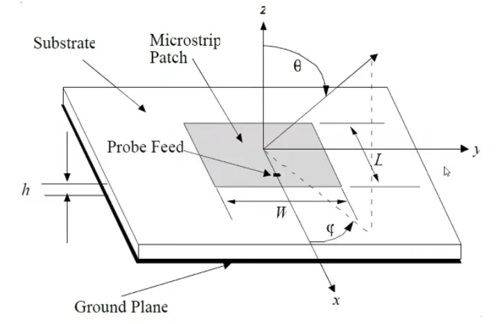
Modern high-precision GNSS antennas for automotive applications typically use a multi-feed patch or crossed-slot architecture on a multilayer PCB. The radiating element may be a ceramic patch, a printed patch, or a crossed-slot structure, but the feed network is universally implemented on the PCB.
A four-feed design is the most common configuration for RTK-grade antennas. Four feed points are placed at 0°, 90°, 180°, and 270° around the radiating element center. A feed network — typically a combination of quarter-wave transformers, impedance matching sections, and a 90° hybrid coupler or phase-shifting network — delivers the received signal from all four feeds to a single output port with the correct amplitude and phase relationships.
The phase center of the antenna is the point in space from which the radiated fields appear to originate. For a perfectly symmetric four-feed patch, the phase center coincides with the geometric center of the patch. Any asymmetry in the feed network — whether in trace length, trace width, or dielectric properties beneath the traces — shifts the effective phase center away from the geometric center. The magnitude of this shift depends on the degree of asymmetry and the operating wavelength.
2.2 Why Phase Center Stability Matters for Automotive RTK
In a static surveying application, a stable but offset phase center can be calibrated out. The antenna's phase center offset is a known, repeatable quantity that can be measured in an anechoic chamber and corrected in software.
In an automotive application, this calibration approach breaks down for three reasons:
Temperature variation. The antenna operates from -40°C to +105°C in the vehicle environment. If the phase center offset changes with temperature — because the dielectric constant of the PCB changes, because the board warps, or because the feed network's electrical length shifts — the calibration becomes invalid. The RTK solution degrades or loses lock.
Mechanical stress. The antenna is mounted on the vehicle roof, where it experiences vibration, thermal cycling, and mechanical stress from the mounting structure. If the PCB warps or deforms under these stresses, the phase center shifts.
Multi-band operation. The antenna must maintain phase center consistency across L1 (1.575 GHz), L2 (1.227 GHz), and L5 (1.176 GHz) — or their equivalents in other constellations. A feed network that is symmetric at one frequency may not be symmetric at another if the dielectric properties vary with frequency or if the trace geometries are not scaled correctly.
For these reasons, automotive GNSS antenna PCBs must be designed and manufactured such that the phase center remains stable in situ, under the full range of environmental and mechanical conditions the vehicle will experience. This requires control of the PCB's mechanical and electrical symmetry at a level that standard commercial PCB manufacturing does not provide.
3. Lamination Symmetry: The Mechanical Foundation of Phase Center Stability
3.1 The Symmetric Stack-Up Principle
A symmetric PCB stack-up is one in which the materials, thicknesses, and copper densities are mirrored about the board's center plane. In a symmetric stack-up, identical materials and thicknesses exist above and below the center axis. During cool-down after lamination, the residual stresses on the top half are mirror images of the bottom half, and the net bending moment is zero.
The alternative — an asymmetric stack-up — produces a net bending moment when the board cools from lamination temperature. This moment causes the board to warp (bow or twist). The warpage may be visible (a few millimeters of bow across a 100 mm board) or microscopic (tens of micrometers), but it is always present to some degree.
For a GNSS antenna PCB, warpage is not merely a cosmetic or assembly issue. It directly shifts the phase center.
3.2 The Warpage-Phase Center Connection
A warped antenna PCB is no longer planar. The radiating patch sits on a curved surface rather than a flat one. The ground plane beneath the feed network is also curved. The distance from the feed network traces to the ground plane varies across the board — and that distance determines the characteristic impedance and electrical length of the feed lines.
For a four-feed antenna, the critical parameter is not the absolute electrical length of each feed line but the difference in electrical length between the four paths. If the board warps symmetrically — a uniform bow — all four feed lines experience similar changes, and the net effect partially cancels. But real warpage is rarely symmetric. It is a combination of bow (cylindrical curvature) and twist (saddle-shaped deformation), and it produces differential changes in the four feed paths.
The phase error introduced by warpage can be estimated. For a feed network operating at 1.575 GHz (L1), the wavelength in the PCB dielectric (Dk ≈ 3.5) is approximately 101 mm. A 1° phase error corresponds to a path length difference of approximately 0.28 mm. If warpage introduces a differential path length of 0.1 mm between two feed lines — a realistic number for a board with 50 μm of bow — the phase error is approximately 0.36°. Over a four-feed network, the resulting phase center shift can exceed 1 mm.
3.3 What Makes a Stack-Up Symmetric
Achieving a symmetric stack-up requires attention to several parameters, all of which must be mirrored about the board center plane:
- Dielectric thickness: The total dielectric thickness above and below the center must be identical, or nearly so. Prepreg plies and core thicknesses must be matched.
- Buildup of the dielectric: The sequence of prepreg and core layers must be mirrored. Using identical prepreg plies at mirror-image locations is highly recommended.
- Pattern density: The copper coverage on each layer must be balanced. If one layer has 80% copper coverage and its mirror-image layer has 50%, the resin flow during lamination will differ, creating stress asymmetry.
- Copper foil thickness: The copper weight on mirror-image layers must be identical. Mixing 1 oz and 0.5 oz copper on mirror-image layers creates CTE mismatch and residual stress.
- Number of layers: The total layer count must be even (or the center must fall on a core, not a prepreg).
The use of thieving pads — small isolated copper features added to low-copper-density areas — can help balance pattern density across a layer and between mirror-image layers.
3.4 The Hybrid Stack-Up Challenge
Many GNSS antenna PCBs use hybrid stack-ups: a low-loss RF material (Rogers RO4000 series, Taconic, or PTFE) for the antenna and feed layers, combined with standard FR-4 for the DC, ground, and control layers. Hybrid stack-ups are attractive for cost reasons, but they complicate symmetry.
The different materials have different CTEs. Rogers RO4350B has a Z-axis CTE of approximately 30–50 ppm/°C; FR-4 has 50–70 ppm/°C. The X-Y CTE also differs. When the board cools from lamination, these CTE differences produce different amounts of shrinkage in the RF and FR-4 regions, creating additional stress and warpage beyond what a homogeneous stack-up would experience.
Industry experience confirms that mixed-substrate PCBs are “not as easy as it appears,” and that hybrid constructions are recommended only on an exception basis. For GNSS antenna PCBs requiring phase center stability below 0.5 mm, the designer should carefully evaluate whether a homogeneous RF stack-up — despite its higher material cost — offers better manufacturing yield and thermal stability than a hybrid approach.
4. Copper Thickness Tolerance: The Electrical Asymmetry Driver
4.1 How Copper Thickness Affects Phase Center
If lamination symmetry determines the mechanical flatness of the board, copper thickness tolerance determines the electrical symmetry of the feed network. The two mechanisms are complementary: lamination asymmetry creates a geometric phase error, while copper thickness variation creates an electrical phase error.
Copper foil thickness in PCB manufacturing is specified with a tolerance of approximately ±10% . For 1 oz (35 μm) copper, the actual thickness ranges from 31.5 μm to 38.5 μm. For ½ oz (17.5 μm) copper, the range is 15.75 μm to 19.25 μm. This variation arises from the foil manufacturing process and is not tightly controlled by most PCB fabricators.
In a GNSS antenna feed network, the copper thickness affects two critical parameters:
Characteristic impedance. The impedance of a microstrip or stripline trace depends on the trace width, the dielectric thickness, and — to a lesser extent — the copper thickness. A ±10% variation in copper thickness shifts the impedance by approximately ±0.5–1.0 Ω for a typical 50Ω trace. This impedance shift, while small, changes the electrical length of the feed line because the propagation velocity is affected by the impedance.
Conductor loss. Thicker copper has lower sheet resistance and therefore lower insertion loss. In a four-feed network, if one feed path has 38 μm copper and another has 32 μm, the insertion loss differs by approximately 0.05–0.1 dB at L1. This amplitude imbalance between feeds translates directly into phase center offset — an amplitude imbalance of 0.1 dB between opposite feeds shifts the phase center by approximately 0.2–0.3 mm.
4.2 The Feed Network Symmetry Problem
The phase center of a multi-feed antenna is determined by the amplitude and phase balance between the feed paths. For a four-feed network with a 90° hybrid combiner, the ideal condition is:
- Equal amplitude on all four feeds
- Exactly 90° phase difference between adjacent feeds (0°, 90°, 180°, 270°)
Any deviation from this ideal condition shifts the phase center. The phase shift from amplitude imbalance is approximately:
Δφ ≈ (ΔA / A) × (180° / π)
where ΔA/A is the fractional amplitude imbalance. For a 0.1 dB imbalance (ΔA/A ≈ 0.023), the phase shift is approximately 1.3°. For a 0.2 dB imbalance, it is 2.6°.
Copper thickness tolerance contributes directly to amplitude imbalance because it changes the conductor loss of each feed path. If the feed network is designed with equal trace lengths and equal geometries, the amplitude imbalance is zero in the ideal case. But if the copper thickness varies across the board — or if the four feed paths are fabricated with different copper thicknesses due to panel position — the amplitude balance degrades.
4.3 The High-Precision Antenna Benchmark
High-precision GNSS antenna manufacturers have recognized the importance of copper thickness control. Industry practice for RTK-grade antennas specifies copper foil thickness in the range of 0.03–0.05 mm (approximately 1–1.4 oz) with tight tolerance control, ensuring uniform signal conduction and reducing phase deviation caused by material non-uniformity. The feed network layout is designed with strict symmetry, placing feed points directly below the geometric center so that phase differences between signals from different directions are controlled within 0.1°.
This level of control — 0.1° phase difference between feeds — requires copper thickness uniformity far tighter than the ±10% standard. It requires a copper thickness tolerance of approximately ±3–5% , or absolute control of ±1 μm for 17.5 μm foil.
5. Quantifying the Combined Impact
The phase center shift from lamination asymmetry and copper thickness tolerance is not additive in a simple linear sense — the two mechanisms interact. But for design purposes, they can be treated as independent contributions to a total error budget.
| Error Source | Typical Contribution | Controlled Contribution | Improvement Factor |
|---|---|---|---|
| Lamination asymmetry (warpage) | 0.8–1.5 mm | 0.2–0.4 mm | 3–4× |
| Copper thickness tolerance (±10%) | 0.3–0.6 mm | 0.05–0.15 mm (±3%) | 4–6× |
| Feed network trace length tolerance | 0.2–0.5 mm | 0.05–0.1 mm | 4–5× |
| Dielectric Dk uniformity | 0.1–0.3 mm | 0.05–0.1 mm | 2–3× |
| Combined (RSS) | 0.9–1.7 mm | 0.25–0.45 mm | 3–4× |
The table shows that with standard commercial tolerances, the combined phase center variation can exceed 1.5 mm — far beyond the 0.5 mm requirement for RTK positioning. With controlled lamination symmetry, copper thickness tolerance, and feed network geometry, the combined variation can be reduced to below 0.5 mm, meeting the RTK requirement with margin.
The dominant contributors are lamination asymmetry and copper thickness tolerance. Dielectric Dk uniformity — which many designers focus on because it is the most visible material specification — is actually the least significant contributor when the stack-up is symmetric and the copper thickness is controlled.
6. Design and Manufacturing Guidelines
6.1 Stack-Up Design for Symmetry
- Use an even layer count with the center plane falling on a core, not a prepreg.
- Mirror dielectric thicknesses exactly above and below the center. Total dielectric thickness above must equal total below within ±5%.
- Mirror copper weights on all mirror-image layers. Do not mix 1 oz and 0.5 oz copper on opposite sides of the center.
- Balance pattern density across each layer. Use thieving pads to bring low-density areas up to the average.
- Minimize hybrid material transitions. If hybrid is unavoidable, place the RF layers symmetrically about the center.
6.2 Copper Thickness Specification
- Specify copper thickness tolerance of ±5% or better for RF and feed network layers. For ½ oz (17.5 μm) copper, this is ±0.9 μm.
- Require copper thickness verification per IPC-TM-650 2.2.13 on every production lot.
- Use the same copper foil lot for all feed network layers to minimize lot-to-lot variation.
6.3 Feed Network Layout
- Route all four feed paths with identical geometry — same trace width, same length, same number of bends, same ground clearance.
- Use arc corners (not 45° or 90° corners) in the feed network to ensure electrical length symmetry.
- Place feed points at exactly 90° intervals around the radiating element center. Measure and verify.
- Avoid vias in the feed network unless absolutely necessary. If vias are required, use identical via configurations on all four paths.
6.4 Lamination Process Control
- Use a lamination profile optimized for the specific stack-up. Ramp rate, pressure, and cool-down rate all affect residual stress.
- Verify board flatness after lamination per IPC-6012 (bow and twist <0.75%). For antenna PCBs, require <0.3%.
- Measure board flatness across temperature (-40°C to +105°C) if possible. A board that is flat at room temperature may warp at temperature extremes.
6.5 Testing and Verification
- Include phase center test structures on the production panel. A small patch antenna with the same feed network geometry can be measured in an anechoic chamber or with a near-field scanner.
- Verify feed network symmetry by measuring S-parameters (S21, S31, S41) of the four feed paths. Amplitude imbalance should be <0.1 dB; phase imbalance should be <2°.
- Perform thermal cycling and re-measure phase center after cycling. Phase center shift after 100 cycles from -40°C to +105°C should be <0.2 mm.
7. Symmetry and Thickness, Not Dk Alone
Automotive GNSS antenna PCBs for RTK positioning require phase center stability below 0.5 mm. The dominant contributors to phase center variation are not dielectric constant uniformity — the parameter most designers focus on — but lamination symmetry and copper thickness tolerance.
- Lamination asymmetry creates board warpage, which introduces differential electrical length errors in the feed network. A board with 50 μm of bow can shift the phase center by 1 mm or more.
- Copper thickness tolerance (±10% standard) creates amplitude imbalance between feed paths, which translates directly into phase center offset. Tightening copper thickness control to ±3% reduces this contribution by 4–6×.
- Feed network geometry must be identical on all four paths — same trace width, same length, same ground clearance, same corner geometry.
- Manufacturing controls — symmetric stack-up, tight copper thickness verification, optimized lamination profile, flatness measurement — are essential for achieving sub-0.5 mm phase center variation in production.
A GNSS antenna PCB designed with a symmetric stack-up, ±3% copper thickness tolerance, and identical feed network geometry will achieve the phase center stability that RTK positioning requires. A design that focuses only on dielectric material selection, while accepting standard lamination and copper tolerances, will measure phase center variation of 1 mm or more — insufficient for centimeter-level positioning, and a source of intermittent RTK degradation that is difficult to diagnose.
8. Frequently Asked Questions
Q1: What is phase center stability and why does it matter for automotive GNSS?
A: Phase center stability is the consistency of the antenna's effective phase reference point across elevation, azimuth, frequency, and temperature. For RTK positioning, phase center variation must be below 0.5 mm. A 1 mm shift produces 0.1° angular error at 1,000 meters, degrading positioning accuracy.
Q2: Why does lamination symmetry affect phase center stability?
A: An asymmetric stack-up creates residual stress that warps the board. Warpage changes the distance from feed network traces to the ground plane, altering electrical length. Differential changes between the four feed paths shift the phase center. A symmetric stack-up minimizes warpage and preserves feed path balance.
Q3: How much copper thickness variation is acceptable for GNSS antenna PCBs?
A: Standard PCB copper thickness tolerance is ±10%, which produces 0.3–0.6 mm of phase center variation. For RTK-grade antennas, specify ±3–5% (±0.5–0.9 μm for ½ oz copper). This reduces the phase center contribution to 0.05–0.15 mm.
Q4: What stack-up parameters must be symmetric?
A: Dielectric thickness, buildup sequence (prepreg/core order), pattern density (copper coverage per layer), copper foil thickness on mirror-image layers, and total layer count. All must be mirrored about the board center plane.
Q5: Can a hybrid stack-up (RF material + FR4) achieve phase center stability below 0.5 mm?
A: It is possible but more difficult. The CTE mismatch between RF material and FR4 creates additional warpage that is not present in a homogeneous stack-up. If hybrid is required, place the RF layers symmetrically about the center and verify flatness across temperature.
Q6: What is the feed network symmetry requirement for phase center stability?
A: All four feed paths must have identical trace width, length, number of bends, ground clearance, and corner geometry. Amplitude imbalance should be <0.1 dB; phase imbalance <2°. This ensures the phase center remains at the geometric center.
Q7: Why is dielectric Dk uniformity less important than lamination symmetry and copper thickness?
A: Dk uniformity affects the absolute electrical length of the feed paths, but if all four paths experience the same Dk, the phase center does not shift. Lamination asymmetry and copper thickness variation create differential errors between paths — these are the mechanisms that actually shift the phase center.
Q8: How do I verify phase center stability in production?
A: Include a phase center test structure on the production panel. Measure feed network S-parameters to verify amplitude and phase balance. Perform thermal cycling and re-measure. For critical programs, request anechoic chamber measurement of a sample from each lot.
Q9: What board flatness specification should I require for GNSS antenna PCBs?
A: IPC-6012 requires bow and twist <0.75%. For antenna PCBs, require <0.3%. Measure flatness after lamination and after thermal cycling to ensure stability across the operating temperature range.
Q10: Does copper thickness affect phase center through impedance or through loss?
A: Both. Copper thickness affects characteristic impedance (through conductor geometry) and insertion loss (through sheet resistance). The impedance effect is smaller but affects electrical length; the loss effect creates amplitude imbalance between feeds, which directly shifts the phase center.
9. About Richfulljoy
Richfulljoy specializes in high-precision RF and antenna PCB manufacturing for automotive GNSS, RTK positioning, and safety-critical applications. Our engineering team understands that phase center stability is determined by manufacturing symmetry — not material selection alone.