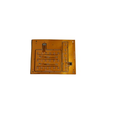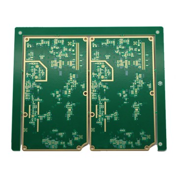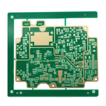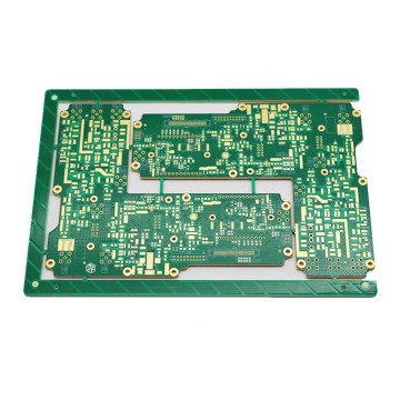

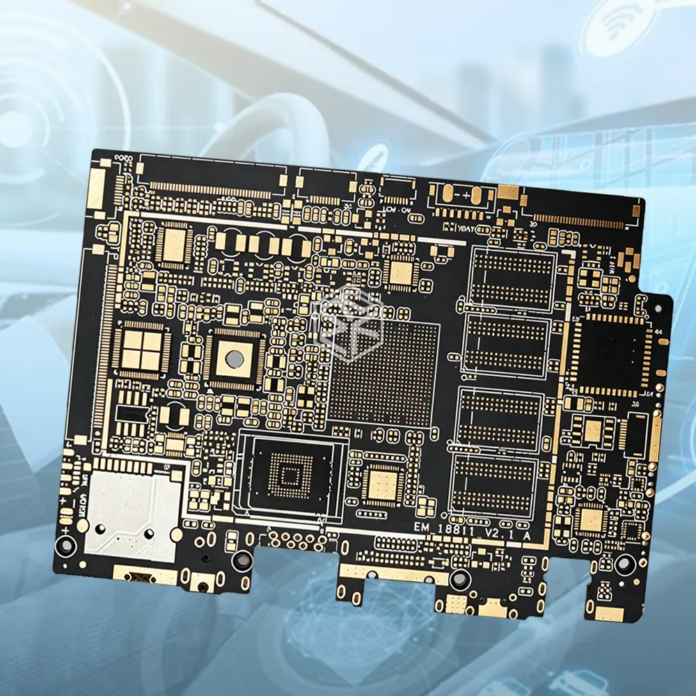
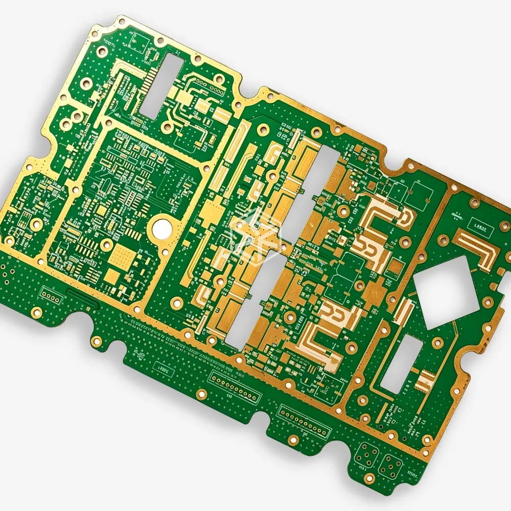
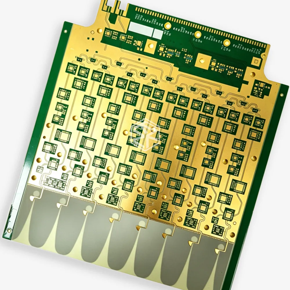
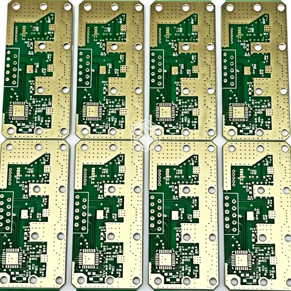
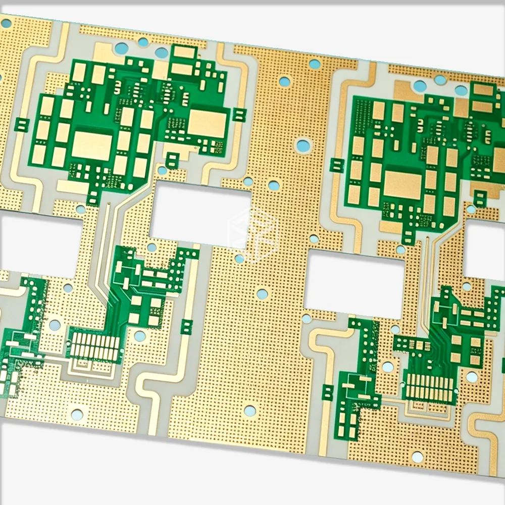
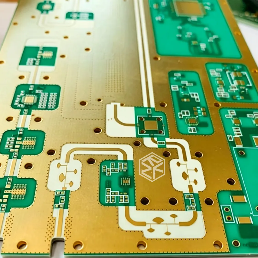
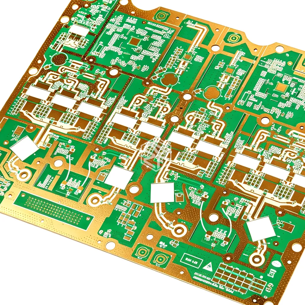
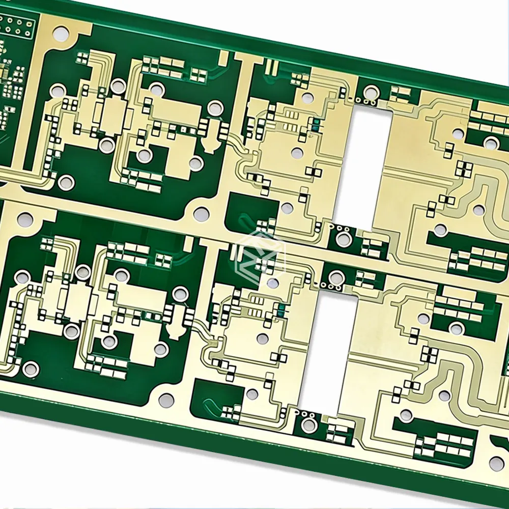
PCB for Inter-Satellite Laser Communication: Mixed Board Design for High-Speed Signals and High-Frequency RF
1. The Convergence of Two Signal Domains
Inter-satellite laser communication is rapidly becoming the backbone of next-generation satellite constellations. By transmitting data via modulated laser beams instead of radio waves, laser crosslinks offer orders-of-magnitude higher bandwidth, lower latency, and inherent security advantages over traditional RF links. Mega-constellations for broadband internet, Earth observation, and defense applications are increasingly relying on optical inter-satellite links to move data across the globe.
Inside every laser communication terminal lies a sophisticated electronic subsystem. It includes high-speed digital processors for encoding, decoding, and error correction; high-frequency RF circuits for driving electro-optic modulators; analog front-ends for photodetector signal recovery; and power management circuitry. All of these functions must be integrated onto a small number of printed circuit boards that operate reliably in the harsh space environment.
The PCB at the heart of this system faces a unique challenge: it must simultaneously handle high-speed digital signals — often exceeding 10 Gbps, 25 Gbps, or even 56 Gbps per lane — and high-frequency RF signals — typically in the Ka-band (26.5–40 GHz), V-band (40–75 GHz), or even W-band (75–110 GHz) for modulator drivers. These two signal domains have different, sometimes conflicting, requirements for materials, stack-up, layout, and manufacturing.
This article examines the design and manufacturing considerations for mixed high-speed and high-frequency RF PCBs used in inter-satellite laser communication terminals.
2. The Dual Requirements: High-Speed Digital and High-Frequency RF
2.1 High-Speed Digital Signals
The digital section of a laser communication terminal processes data at multi-gigabit rates. Typical interfaces include:
- SerDes lanes at 10–56 Gbps per lane, often using PAM4 modulation
- High-speed serial interfaces such as JESD204B/C for ADC/DAC connections
- Memory interfaces (DDR4, DDR5) for buffering and processing
- Low-voltage differential signaling (LVDS) for control and telemetry
High-speed digital signals are characterized by their broad frequency spectrum. A 25 Gbps NRZ signal has significant energy up to 12.5 GHz; a 56 Gbps PAM4 signal extends beyond 28 GHz. The PCB must maintain signal integrity across this entire spectrum — controlling impedance, minimizing crosstalk, and managing losses.
2.2 High-Frequency RF Signals
The RF section drives the electro-optic modulator and processes signals from the photodetector. Typical frequencies include:
- Modulator driver output: 20–40 GHz (Ka-band) or higher
- Photodetector output: DC to 40 GHz, often with low-noise amplification
- Local oscillator distribution: 10–30 GHz
- RF filtering and matching networks: Application-specific
RF signals require low insertion loss, high isolation, and stable impedance across a narrow but critical frequency band. They are sensitive to material losses, connector transitions, and ground plane discontinuities.
2.3 The Frequency Overlap
The critical observation is that the digital and RF frequency spectra overlap. A 56 Gbps PAM4 digital signal has significant energy at 28 GHz — the same frequency used for some RF modulator drivers. The PCB must handle both signal types without compromising either.
This overlap creates a shared requirement: the PCB material must have low loss at frequencies from DC to 40 GHz or higher. But it also creates a conflict: high-speed digital signals are sensitive to impedance discontinuities and crosstalk, while RF signals are sensitive to isolation and phase stability. The layout must satisfy both.
3. Material Selection for Mixed-Signal Space PCBs
3.1 The Space-Grade Requirement
Before considering electrical performance, the material must meet the requirements of the space environment:
- Low outgassing: Total mass loss (TML) < 1.0%, collected volatile condensable materials (CVCM) < 0.1% per ASTM E595
- Radiation tolerance: Ability to withstand total ionizing dose (TID) of 50–100 krad or more without significant degradation
- Wide temperature stability: Operation from -55°C to +125°C (or wider for some missions)
- Thermal cycling resistance: Thousands of cycles without delamination or cracking
- Vacuum compatibility: No trapped volatiles that could condense on optical surfaces
Materials that are commonly used in commercial RF PCBs — such as standard FR-4 — are generally not acceptable for space applications due to outgassing and radiation susceptibility. Space-grade materials must be specifically qualified.
3.2 Candidate Materials for Mixed-Signal Space PCBs
| Material | Dk @ 10 GHz | Df @ 10 GHz | Space Qualified? | Application |
|---|---|---|---|---|
| Rogers RO3003 | 3.00 | 0.0010 | Yes (with proper construction) | RF layers, millimeter-wave |
| Rogers RO4350B | 3.48 | 0.0037 | Yes (low outgassing versions) | RF and high-speed digital |
| Panasonic Megtron 6 | 3.7 | 0.0020 | Yes (space-grade versions) | High-speed digital |
| Taconic TLY-5 | 2.2 | 0.0009 | Yes | RF layers, low loss |
| Arlon 85N | 3.2 | 0.0025 | Yes | RF and digital hybrid |
| Polyimide (Kapton-based) | 3.4 | 0.0050 | Yes | Flexible and rigid-flex |
The selection depends on the specific frequency, loss budget, and mechanical requirements. For the RF layers, Rogers RO3003 or Taconic TLY-5 offer the lowest loss. For high-speed digital layers, Megtron 6 or RO4350B provide a balance of low loss and manufacturability. Polyimide is used where flexible or rigid-flex construction is required.
3.3 Hybrid Stack-Ups
A typical mixed-signal space PCB might use:
- RF layers: Rogers RO3003 or TLY-5 (lowest loss)
- High-speed digital layers: Megtron 6 or RO4350B (low loss, good impedance control)
- Power and ground layers: Space-grade FR-4 or polyimide (cost-effective, adequate for DC and low-frequency)
The challenge is bonding these dissimilar materials together reliably. CTE mismatch, different curing profiles, and different surface energies all complicate the lamination process. The use of compatible prepregs and carefully controlled lamination cycles is essential.
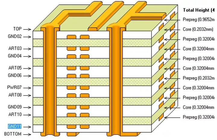
4. Stack-Up Design for Mixed-Signal Space PCBs
4.1 Layer Assignment
A well-designed stack-up separates RF and high-speed digital signals to minimize interference:
- Top layer: RF signal routing (modulator driver, photodetector input)
- Layer 2: Solid ground plane (RF reference)
- Layer 3: High-speed digital routing
- Layer 4: Ground plane
- Layer 5: Power plane
- Layer 6: High-speed digital routing
- Layer 7: Solid ground plane
- Bottom layer: RF signal routing (if needed) or low-speed control
This arrangement places the RF layers on the outside, where they can be isolated by ground planes. The high-speed digital layers are buried between ground planes, which provides shielding and controlled impedance.
4.2 Impedance Control
Both RF and high-speed digital traces require controlled impedance — typically 50Ω single-ended and 100Ω differential. However, the required trace geometries differ:
- RF traces: Often use grounded coplanar waveguide (GCPW) for tight field confinement and low loss
- High-speed digital traces: Often use stripline or microstrip for controlled impedance and routing density
The stack-up must accommodate both. This may require different dielectric thicknesses for RF and digital layers, which complicates the lamination process.
4.3 Ground Plane Strategy
A continuous, low-impedance ground plane is essential for both RF and high-speed digital performance. The ground plane must:
- Provide a consistent reference for controlled impedance
- Minimize return current paths
- Shield RF and digital signals from each other
- Provide thermal paths for heat dissipation
Ground plane splits should be avoided, especially under RF and high-speed traces. If splits are necessary for power isolation, they should be bridged with stitching capacitors or placed away from critical signal paths.
5. Transition Zone Design: From RF to Digital
5.1 The RF-to-Digital Interface
In a laser communication terminal, the RF and digital domains must interface. The modulator driver receives a digital data stream and converts it to an RF signal. The photodetector produces an RF signal that is amplified and then digitized by an ADC. These interfaces require careful design.
At the PCB level, the transition may involve:
- Different materials: RF layer on Rogers, digital layer on Megtron
- Different transmission line types: GCPW on RF, stripline on digital
- Different connectors: SMPM or 2.92mm for RF, high-density connectors for digital
Each transition introduces impedance discontinuities that must be minimized.
5.2 Via Transitions
Vias are often used to route signals between layers. In a mixed-signal space PCB, vias must be designed to:
- Maintain controlled impedance through the transition
- Minimize parasitic inductance and capacitance
- Provide a return path for the signal
For RF signals, backdrilling is often necessary to remove via stubs that would otherwise create resonances. For high-speed digital signals, via stubs can also degrade signal integrity, though the tolerance is somewhat greater.
Ground vias should be placed around signal vias to provide a consistent return path and reduce crosstalk.
5.3 Material Transition
When a signal transitions from one material to another (e.g., from Rogers to Megtron), the effective dielectric constant changes, which changes the impedance. The trace geometry must be adjusted to compensate. A gradual taper over several wavelengths is preferred to an abrupt step.
The transition zone should be kept as short as possible and should be fully characterized through electromagnetic simulation.
6. Signal Integrity and Power Integrity
6.1 Signal Integrity Challenges
Insertion loss: At 28 GHz, the insertion loss of a 50Ω microstrip line on Rogers RO3003 is approximately 0.15 dB/cm. On Megtron 6, it is approximately 0.25 dB/cm. The total loss budget must account for trace length, connectors, and transitions.
Crosstalk: High-speed digital traces can couple into RF traces, and vice versa. Maintaining adequate spacing, using ground planes for shielding, and routing orthogonally can minimize crosstalk.
Jitter: In high-speed digital links, jitter is a critical parameter. Material losses, impedance discontinuities, and crosstalk all contribute to jitter. Low-loss materials and careful layout minimize jitter.
Phase stability: RF signals used for modulator driving require stable phase. Temperature changes cause Dk to change, which changes propagation delay. Materials with low TCDk (like RO3003 at -3 ppm/°C) minimize phase drift.
6.2 Power Integrity Challenges
The laser communication terminal contains sensitive RF and high-speed digital circuits that are vulnerable to power supply noise. Power integrity design must:
- Provide low-noise power to RF and analog circuits
- Minimize simultaneous switching noise (SSN) from digital circuits
- Maintain stable voltage under dynamic load conditions
Techniques include:
- Multiple decoupling capacitors (10 pF to 100 μF) placed close to load points
- Low-noise LDOs for RF and analog power
- Power plane segmentation to isolate noisy digital power from sensitive RF power
- Ferrite beads to filter high-frequency noise
7. Thermal Management in the Space Environment
In space, there is no air convection. Heat must be conducted to the satellite structure and radiated to space. The PCB plays a critical role in thermal management.
7.1 Thermal Paths
- Thermal vias: Arrays of vias under high-power components (modulator drivers, amplifiers) conduct heat to internal copper planes
- Copper planes: Ground and power planes spread heat laterally
- Metal core or heat sink: For very high-power components, a metal core or attached heat sink may be required
7.2 CTE Matching
The PCB materials must have compatible coefficients of thermal expansion to avoid delamination or cracking during thermal cycling. The CTE of the dielectric materials, copper, and any metal core must be considered. Polyimide and some space-grade epoxies have CTEs closer to copper than standard FR-4.
8. Space Environment Reliability
8.1 Radiation Effects
Satellites in low Earth orbit (LEO) experience total ionizing dose (TID) of 10–100 krad over a 5–10 year mission. Geostationary orbit (GEO) and deep space missions experience higher doses. The PCB materials must withstand this radiation without significant degradation of dielectric properties or mechanical integrity.
Single-event effects (SEE) — including single-event upset (SEU) and single-event latch-up (SEL) — are caused by energetic particles. While SEE primarily affects active components, the PCB layout can influence susceptibility by affecting signal integrity and power distribution.
8.2 Outgassing
In vacuum, materials release trapped volatiles. These volatiles can condense on sensitive surfaces — including optical components — degrading performance. Materials must meet ASTM E595 requirements for low outgassing.
8.3 Thermal Cycling
Satellites experience thousands of thermal cycles over their mission life. Each cycle stresses the PCB due to CTE mismatch between materials. Delamination, via cracking, and solder joint fatigue are the primary failure modes. Proper material selection, lamination control, and design margins are essential.
8.4 Vibration and Shock
Launch and deployment subject the PCB to severe vibration and shock. Mechanical design must ensure that components and board-level attachments survive. Conformal coating, staking, and mechanical reinforcement are common techniques.
9. Manufacturing Considerations for Space-Grade Mixed-Signal PCBs
Manufacturing space-grade PCBs requires capabilities beyond standard commercial fabrication:
- Material handling: Space-grade materials require careful storage and handling to prevent contamination
- Lamination control: Hybrid stack-ups require precise control of temperature, pressure, and cure profile
- Registration accuracy: Tight layer-to-layer registration (±2 mil or better) is essential for impedance control and via reliability
- Cleanliness: Ionic contamination must be minimized to prevent corrosion and leakage
- Testing: Full electrical test, impedance verification, thermal cycling, and outgassing certification are required
- Documentation: Full traceability, material certifications, and process records are mandatory
Standards such as IPC-6012 Class 3, NASA-STD-8739, and ESA ECSS-Q-ST-70-08 provide the framework for space-grade PCB qualification.
10. Summary: The Mixed-Signal Challenge
Inter-satellite laser communication terminals demand PCBs that handle both high-speed digital signals and high-frequency RF signals in the harsh space environment. The design and manufacturing challenges are significant:
- Material selection must balance low loss, low outgassing, radiation tolerance, and thermal stability
- Hybrid stack-ups combine different materials for RF, digital, and power layers
- Transition zones between materials and between signal domains require careful design
- Signal integrity must be maintained across the overlapping frequency spectra of digital and RF signals
- Power integrity must isolate sensitive RF circuits from noisy digital circuits
- Thermal management must conduct heat in the absence of convection
- Space environment reliability requires radiation tolerance, low outgassing, and thermal cycling endurance
- Manufacturing must meet space-grade quality and documentation standards
A well-designed mixed-signal space PCB will enable reliable, high-performance laser communication links. A design that ignores the unique requirements of the space environment or the interaction between digital and RF domains may pass initial testing but fail in orbit — where repair is impossible.
11. Frequently Asked Questions
Q1: What makes inter-satellite laser communication PCBs different from standard RF PCBs?
A: They must handle both high-speed digital signals (multi-gigabit SerDes) and high-frequency RF signals (Ka/V/W-band) on the same board, while also meeting space-grade requirements for outgassing, radiation tolerance, and thermal cycling.
Q2: Can standard FR-4 be used for space laser communication PCBs?
A: Generally no. Standard FR-4 has high outgassing and poor radiation tolerance. Space-grade materials — such as Rogers RO3003, Megtron 6, or polyimide — are required for critical RF and high-speed digital layers.
Q3: What is the most critical design challenge in a mixed-signal space PCB?
A: The transition zones — between different materials (RF vs. digital) and between different signal domains. Impedance discontinuities at these transitions can degrade both RF and high-speed digital performance.
Q4: How do you control impedance in a hybrid stack-up?
A: Trace geometries must be adjusted for the different dielectric constants of the materials. Gradual tapering and full-wave electromagnetic simulation are used to design transitions that maintain 50Ω or 100Ω impedance.
Q5: Why is backdrilling important for space RF PCBs?
A: Backdrilling removes unused via stubs that cause resonances at high frequencies. For RF signals in the Ka-band and above, via stubs can severely degrade insertion loss and return loss.
Q6: What thermal management techniques are used in space PCBs?
A: Thermal vias, copper planes, metal cores, and attached heat sinks conduct heat to the satellite structure. In the vacuum of space, conduction is the primary heat transfer mechanism.
Q7: How does radiation affect PCB materials?
A: Radiation can degrade dielectric properties, cause embrittlement, and increase outgassing. Space-grade materials are tested for total ionizing dose (TID) tolerance, typically 50–100 krad or more.
Q8: What outgassing standards apply to space PCBs?
A: ASTM E595 requires total mass loss (TML) < 1.0% and collected volatile condensable materials (CVCM) < 0.1%. Materials must be certified to these standards.
Q9: How many thermal cycles must a space PCB survive?
A: Mission-dependent, but typically thousands of cycles from -55°C to +125°C. CTE-matched materials and controlled lamination are essential to prevent delamination and via cracking.
Q10: What testing is required for space-grade mixed-signal PCBs?
A: Full electrical test, impedance verification, thermal cycling, thermal vacuum testing, outgassing certification, and radiation testing (where applicable). Documentation must include full traceability and material certifications.
12. About Richfulljoy
Richfulljoy specializes in high-reliability PCBs for space, aerospace, and defense applications. Our engineering team understands the unique challenges of mixed-signal space PCBs — from material selection to transition zone design to space-grade qualification.