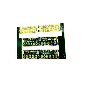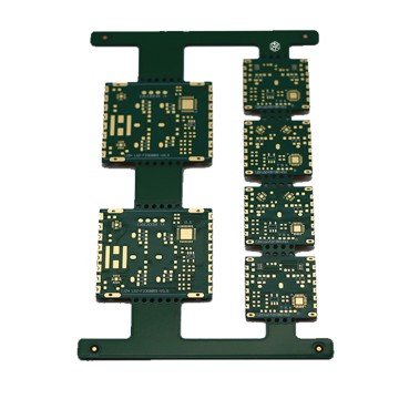

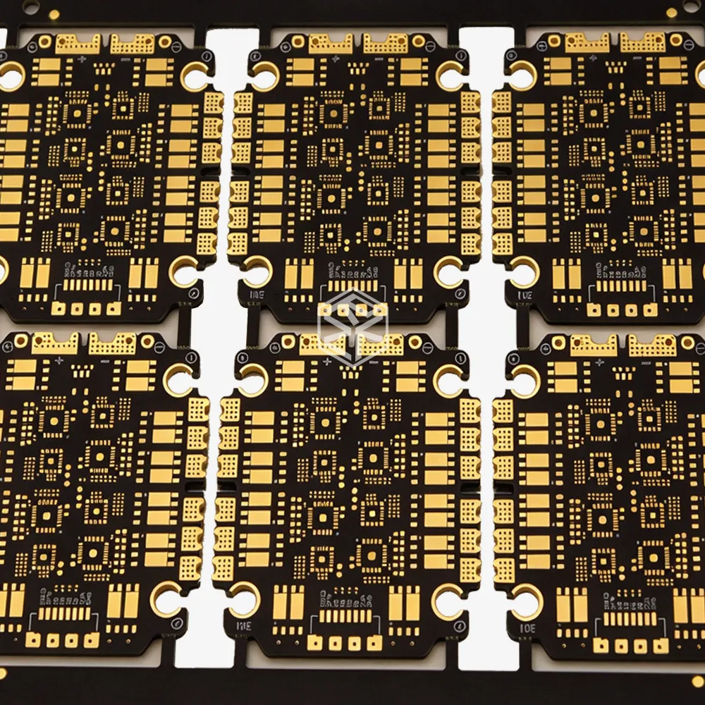
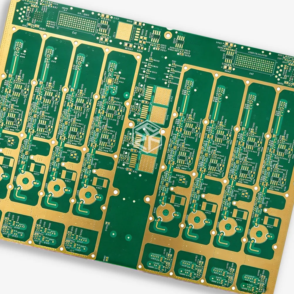
Optical Module Hybrid PCB: Transition Zone Design Between High-Frequency Material and FR4 Is Critical
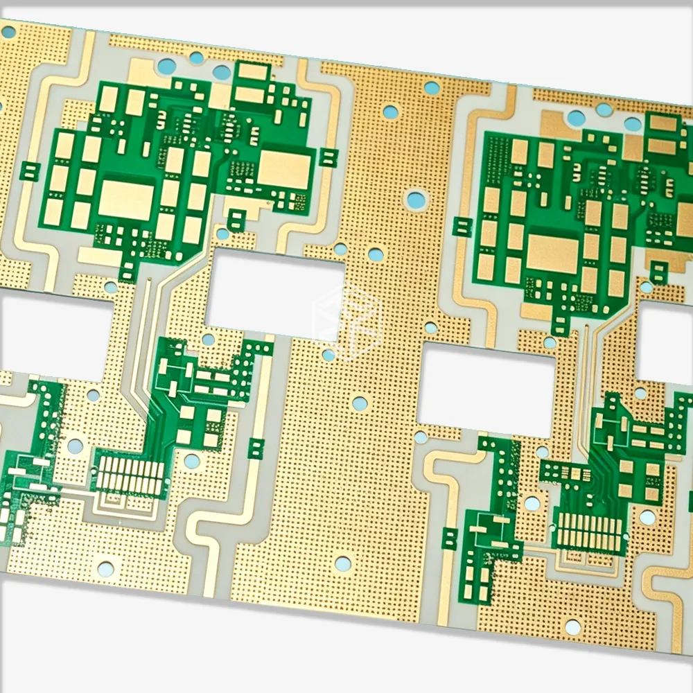
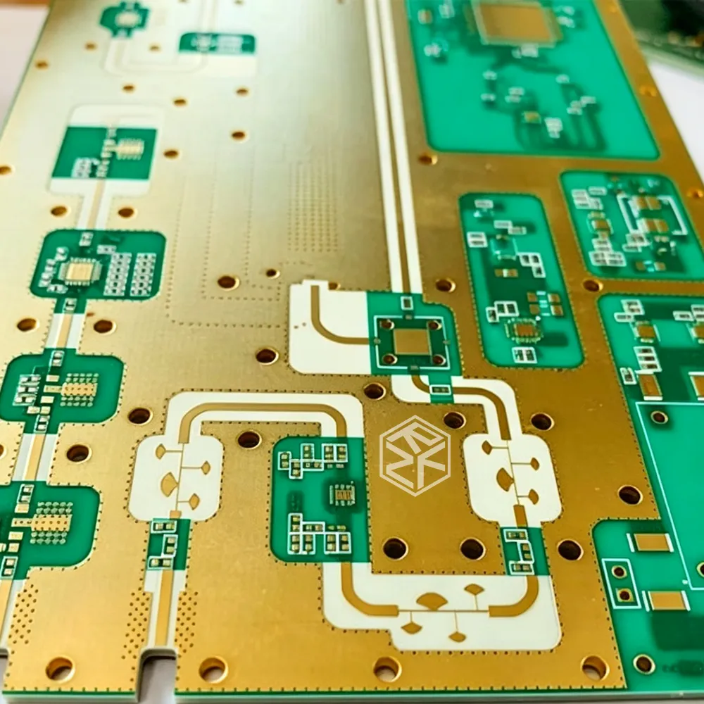
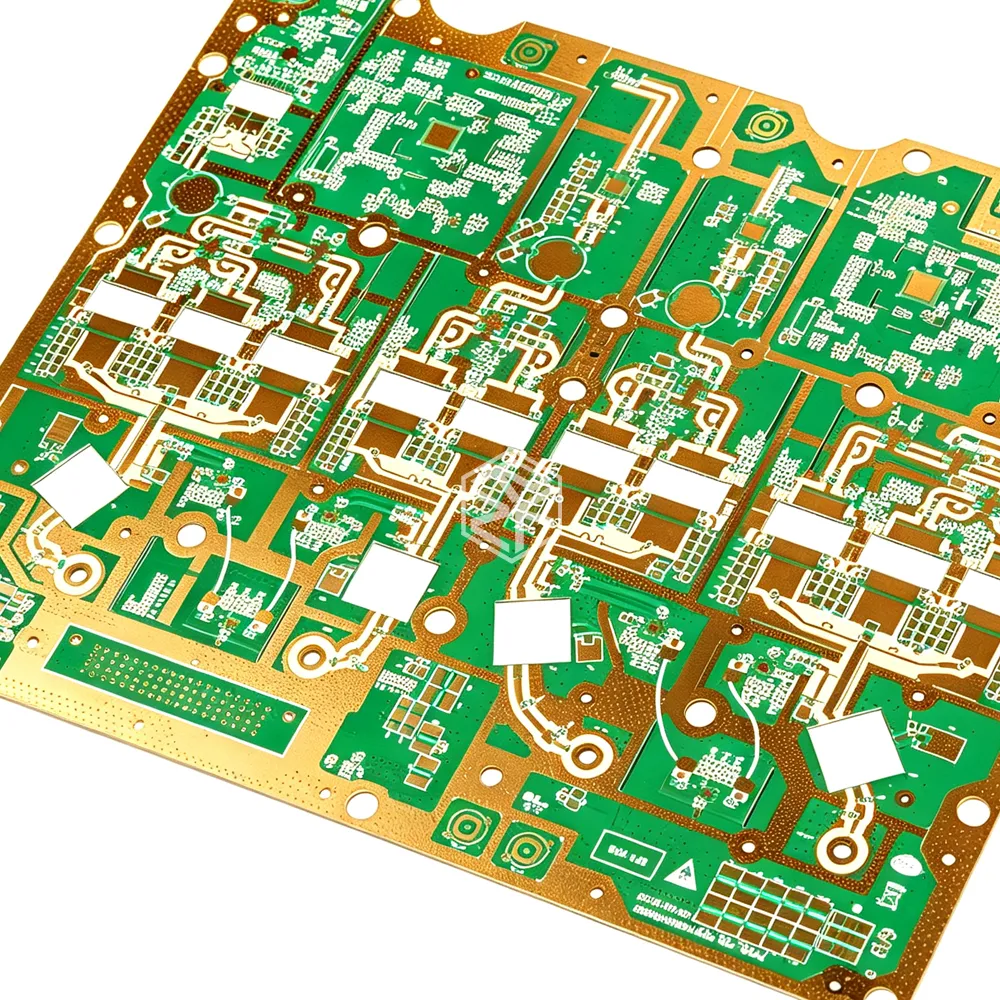
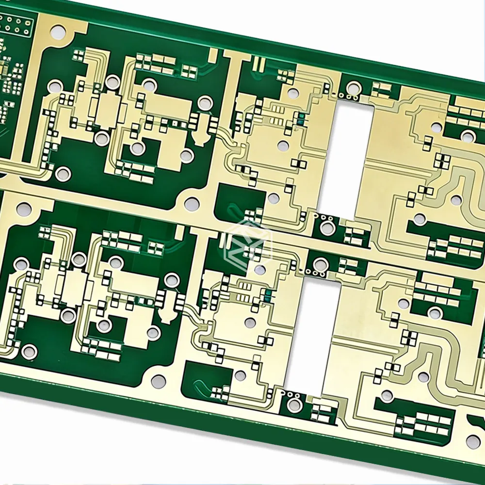
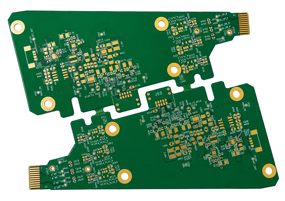
1. The Hybrid Stack-Up That Makes 400G/800G Possible
Optical modules are the workhorses of modern data centers, telecom networks, and high-performance computing. As speeds climb from 100G to 400G, 800G, and beyond, the PCB inside these modules must handle signal frequencies that reach 53 Gbaud (PAM4), 106 Gbaud, and higher — with Nyquist frequencies well into the millimeter-wave range.
A pure high-frequency stack-up — using Rogers, PTFE, or other low-loss materials for every layer — would meet the electrical requirements. But it would also cost 5 to 10 times more than a standard FR-4 board. For high-volume optical module production, that cost is prohibitive.
The solution is the hybrid stack-up: high-frequency material only where it matters — the RF signal layers — and standard FR-4 for the power, ground, and low-speed digital layers. This approach delivers the required electrical performance at a fraction of the cost.
But the hybrid stack-up introduces a critical challenge that pure high-frequency designs do not face: the transition zone between the high-frequency material and the FR4.
At this boundary, the dielectric constant changes, the loss tangent changes, the coefficient of thermal expansion changes, and the mechanical properties change. Every signal that crosses this boundary — and in an optical module, many high-speed signals do — encounters an impedance discontinuity that can degrade signal integrity, increase jitter, and close the eye diagram.
The transition zone is not a detail. It is the critical design feature that determines whether a hybrid optical module PCB meets its performance targets or fails.
2. Why Optical Modules Use Hybrid Stack-Ups
2.1 The Cost-Performance Trade-Off
An 800G optical module might use 8 or 16 lanes of 106 Gbaud PAM4 signaling. The RF traces carrying these signals require:
• Low insertion loss: To maintain signal amplitude over the module's internal routing
• Controlled impedance: To minimize reflections and preserve signal integrity
• Low skew: To maintain timing between differential pairs
• High thermal stability: To perform consistently over the module's operating temperature range
High-frequency materials like Rogers RO3003, RO4350B, or Panasonic Megtron 6 deliver these properties. But they cost significantly more than FR-4. A hybrid stack-up uses these materials only for the layers that carry RF signals, while FR-4 handles the DC power distribution, ground planes, and low-speed control signals.
2.2 The Typical Hybrid Stack-Up
A typical 8-layer hybrid stack-up for an 800G optical module might look like this:
| Layer | Material | Function |
|---|---|---|
| L1 | High-frequency material | RF signal (Tx/Rx) |
| L2 | FR-4 | Ground |
| L3 | FR-4 | Low-speed digital |
| L4 | FR-4 | Power |
| L5 | FR-4 | Power |
| L6 | FR-4 | Low-speed digital |
| L7 | FR-4 | Ground |
| L8 | High-frequency material | RF signal (Tx/Rx) |
The high-frequency material is used only on the outer layers, where the RF signals are routed. The inner layers use FR-4.
The challenge: the RF signal must transition from the high-frequency material at the surface to the FR-4-based inner layers through vias. And in some designs, the RF signal may also transition laterally between high-frequency and FR-4 regions on the same layer.
3. The Transition Zone: Where Two Worlds Meet
3.1 The Dielectric Discontinuity
The most fundamental challenge at the transition zone is the change in dielectric constant.
High-frequency materials typically have Dk values in the range of 3.0 to 3.5. FR-4 has a Dk of 4.2 to 4.8. When a signal crosses from one material to the other, the effective Dk changes abruptly, which changes the propagation velocity and the characteristic impedance.
For a microstrip line, the characteristic impedance is:
Z₀ = √(L/C)
where L and C are the distributed inductance and capacitance. The capacitance is proportional to the dielectric constant. When Dk increases from 3.3 (high-frequency material) to 4.5 (FR-4), the capacitance increases by approximately 36%, and the impedance decreases by approximately 15% — from 50Ω to 42.5Ω.
This impedance discontinuity creates a reflection. The reflection coefficient is:
Γ = (Z₂ - Z₁) / (Z₂ + Z₁) = (42.5 - 50) / (42.5 + 50) = -0.081
A reflection coefficient of -0.081 corresponds to a return loss of approximately -22 dB. While this may seem acceptable at first glance, the cumulative effect of multiple transitions — and the interaction with other discontinuities — can degrade the eye diagram significantly.
3.2 The Loss Tangent Discontinuity
The dielectric loss (tan δ) also changes at the transition. High-frequency materials have tan δ of 0.001 to 0.004; FR-4 has tan δ of 0.02 to 0.05. A signal crossing from high-frequency material into FR-4 experiences a sudden increase in attenuation.
At 28 GHz, the insertion loss of a 50Ω microstrip line on FR-4 can be 0.5 dB/cm or more, compared to 0.1-0.2 dB/cm on Rogers RO4350B. If the transition zone is not carefully designed, the FR-4 section can dominate the total insertion loss of the RF path.
3.3 The CTE Mismatch
High-frequency materials and FR-4 have different coefficients of thermal expansion (CTE). Rogers RO4350B has a Z-axis CTE of approximately 30-50 ppm/°C; FR-4 has a Z-axis CTE of 50-70 ppm/°C. The X-Y CTE also differs.
During thermal cycling — during assembly, during operation, or during environmental testing — this CTE mismatch creates mechanical stress at the transition zone. The stress can cause:
• Delamination at the material interface
• Cracking of plated through-holes or vias near the transition
• Warpage of the board, which shifts the impedance
3.4 The Via Transition
In a hybrid stack-up, the RF signal must often transition vertically through vias — from the high-frequency surface layer to an inner layer, or from one side of the board to the other. These via transitions are additional discontinuities that compound the challenge of the material transition.
A via has its own parasitic inductance and capacitance. When the via also crosses a material boundary, the impedance profile becomes complex, and the reflection can be significant.
4. Design Strategies for the Transition Zone
4.1 Gradual Impedance Transition
The abrupt impedance change at the material boundary can be smoothed by gradually tapering the trace geometry as it approaches the transition. By widening or narrowing the trace in the transition region, the impedance can be kept closer to 50Ω across the boundary.
For a transition from high-frequency material (Dk = 3.3) to FR-4 (Dk = 4.5), the trace width on the FR-4 side must be reduced to maintain 50Ω. A typical rule of thumb is:
• Trace width on high-frequency material: W_hf
• Trace width on FR-4: W_fr4 = W_hf × √(Dk_hf / Dk_fr4) ≈ W_hf × 0.86
A gradual taper over a length of at least 3 to 5 times the trace width reduces the reflection compared to an abrupt step.
4.2 Via Design and Backdrilling
Vias that cross the material boundary must be designed to minimize their parasitic effects:
• Use smaller vias to reduce parasitic capacitance
• Use backdrilling to remove unused via stubs, which cause resonances at high frequencies
• Place ground vias around the signal via to provide a consistent return path and reduce inductance
• Avoid via stubs — any stub longer than λ/20 at the highest frequency of interest will create a resonance
For 106 Gbaud PAM4 signals, backdrilling is often mandatory for via transitions in the RF path.
4.3 Ground Plane Continuity
The ground plane must be continuous across the material boundary. Any gap or discontinuity in the ground plane — particularly at the transition — will disrupt the return current path and create additional reflections.
If the ground plane is on an inner layer that spans both the high-frequency and FR-4 regions, it should be a solid copper plane with no splits or slots in the transition zone.
4.4 Solder Mask and Surface Finish
The surface finish and solder mask can also affect the transition. ENIG is commonly used for optical module PCBs, but at high frequencies, the nickel layer can add loss. For critical RF traces, consider:
• Immersion silver or immersion tin for lower loss
• Selective ENIG only on pads that require soldering
• No solder mask on critical RF traces in the transition zone
4.5 Thermal Management
The CTE mismatch at the transition zone can be managed by:
• Using compatible materials — choose high-frequency materials with CTE closer to FR-4
• Adding stiffeners or thermal vias to distribute mechanical stress
• Controlling the lamination process to minimize residual stress
Table 1 — Transition zone design checklist
| Design Element | Recommendation |
|---|---|
| Impedance taper | Gradual taper over 3–5× trace width |
| Trace width on FR-4 | W_fr4 ≈ W_hf × 0.86 |
| Via design | Small vias, backdrilled, ground vias around signal via |
| Ground plane | Continuous, no splits in transition zone |
| Surface finish | Immersion silver for RF traces; selective ENIG on pads |
| Thermal management | CTE-compatible materials, stiffeners, controlled lamination |
5. Manufacturing Considerations for Hybrid Stack-Ups
5.1 Lamination Process Control
Hybrid stack-ups require careful lamination control. The high-frequency material and FR-4 may have different curing temperatures, resin flow characteristics, and shrinkage rates. The lamination profile must be optimized to ensure proper bonding without damaging either material.
5.2 Registration Accuracy
The transition zone requires precise registration between the high-frequency and FR-4 layers. Misalignment of the ground plane or the signal trace at the boundary can create additional impedance discontinuities.
For 400G/800G optical modules, registration accuracy of ±2 mil (±50 μm) or better is recommended.
5.3 Material Compatibility
Not all high-frequency materials bond well to FR-4. Some materials require special prepregs or surface treatments to achieve adequate adhesion. The fabrication drawing should specify the prepreg type and any surface preparation requirements.
5.4 Testing and Verification
The transition zone should be verified through:
• TDR (Time Domain Reflectometry) to measure the impedance profile across the transition
• VNA (Vector Network Analyzer) to measure S-parameters (return loss, insertion loss)
• Eye diagram measurements to verify signal integrity at the module level
Test coupons that replicate the transition zone geometry should be included on the production panel.
6. Summary: The Transition Zone Is the Critical Design Feature
Hybrid stack-ups are essential for cost-effective 400G/800G optical modules. They deliver the electrical performance of high-frequency materials where it matters, while using FR-4 for the less critical layers.
But the transition zone between high-frequency material and FR-4 introduces impedance discontinuities, loss discontinuities, and mechanical stress that can degrade signal integrity and reliability.
The key takeaways:
• The dielectric constant change from high-frequency material (Dk ~3.3) to FR-4 (Dk ~4.5) creates an impedance drop of ~15% — a reflection coefficient of ~-22 dB
• The loss tangent change increases insertion loss in the FR-4 section
• The CTE mismatch creates mechanical stress that can cause delamination or via cracking
• Gradual impedance tapering, backdrilled vias, and continuous ground planes are essential design strategies
• Manufacturing control — lamination, registration, material compatibility — determines whether the transition performs as designed
• Testing — TDR, VNA, eye diagram — verifies the transition zone performance
A hybrid optical module PCB designed with a well-optimized transition zone will deliver the signal integrity required for 400G/800G. A design that ignores the transition zone may pass initial testing but fail in the field — or fail to meet the eye diagram margin required for reliable operation.
The transition zone is not a detail. It is the critical design feature that determines whether a hybrid stack-up succeeds or fails.
7. Frequently Asked Questions
Q1: Why do optical modules use hybrid stack-ups instead of all high-frequency materials?
A: Cost. A pure high-frequency stack-up costs 5–10× more than a hybrid. Hybrid stack-ups use high-frequency material only on the RF layers and FR-4 on the remaining layers, delivering the required electrical performance at a fraction of the cost.
Q2: What is the main challenge in a hybrid stack-up?
A: The transition zone between the high-frequency material and FR-4. The dielectric constant changes (Dk ~3.3 to ~4.5), the loss tangent changes, and the CTE changes, creating impedance discontinuities and mechanical stress.
Q3: How much does the impedance change at the transition zone?
A: The Dk change from ~3.3 to ~4.5 causes approximately a 15% drop in characteristic impedance — from 50Ω to about 42.5Ω, corresponding to a reflection coefficient of about -0.081 (-22 dB return loss).
Q4: How can the impedance discontinuity be reduced?
A: Use a gradual taper in the trace width as it approaches the transition. Trace width on FR-4 should be approximately 0.86× the width on the high-frequency material. A taper length of at least 3–5× the trace width is recommended.
Q5: Why is backdrilling important in hybrid stack-ups?
A: Backdrilling removes unused via stubs that create resonances at high frequencies. For 106 Gbaud PAM4 signals, backdrilling is often mandatory to maintain signal integrity through via transitions.
Q6: How does CTE mismatch affect the transition zone?
A: The high-frequency material and FR-4 have different coefficients of thermal expansion. During thermal cycling, this mismatch creates mechanical stress that can cause delamination, via cracking, or warpage at the transition boundary.
Q7: What surface finish is recommended for RF traces in optical modules?
A: Immersion silver or immersion tin offers lower loss than ENIG at high frequencies. Selective ENIG should be used only on pads that require soldering. Solder mask should be avoided on critical RF traces in the transition zone.
Q8: What registration accuracy is required for the transition zone?
A: For 400G/800G optical modules, registration accuracy of ±2 mil (±50 μm) or better is recommended to minimize impedance discontinuities at the material boundary.
Q9: How do I verify the transition zone performance?
A: Use TDR to measure the impedance profile across the transition, VNA to measure S-parameters (return loss, insertion loss), and eye diagram measurements to verify signal integrity. Include test coupons that replicate the transition geometry.
Q10: Can FR-4 be used for the RF layers in an optical module?
A: No. FR-4 has too high a loss tangent (0.02–0.05) for RF layers at 400G/800G speeds. High-frequency material is required for the RF signal layers. FR-4 is used only for power, ground, and low-speed digital layers.
8. About Richfulljoy
Richfulljoy specializes in high-performance optical module PCB manufacturing with advanced hybrid stack-up capabilities. Our engineering team understands that the transition zone between high-frequency material and FR-4 is the critical design feature — and we support customers in optimizing it for 400G/800G performance.