


01
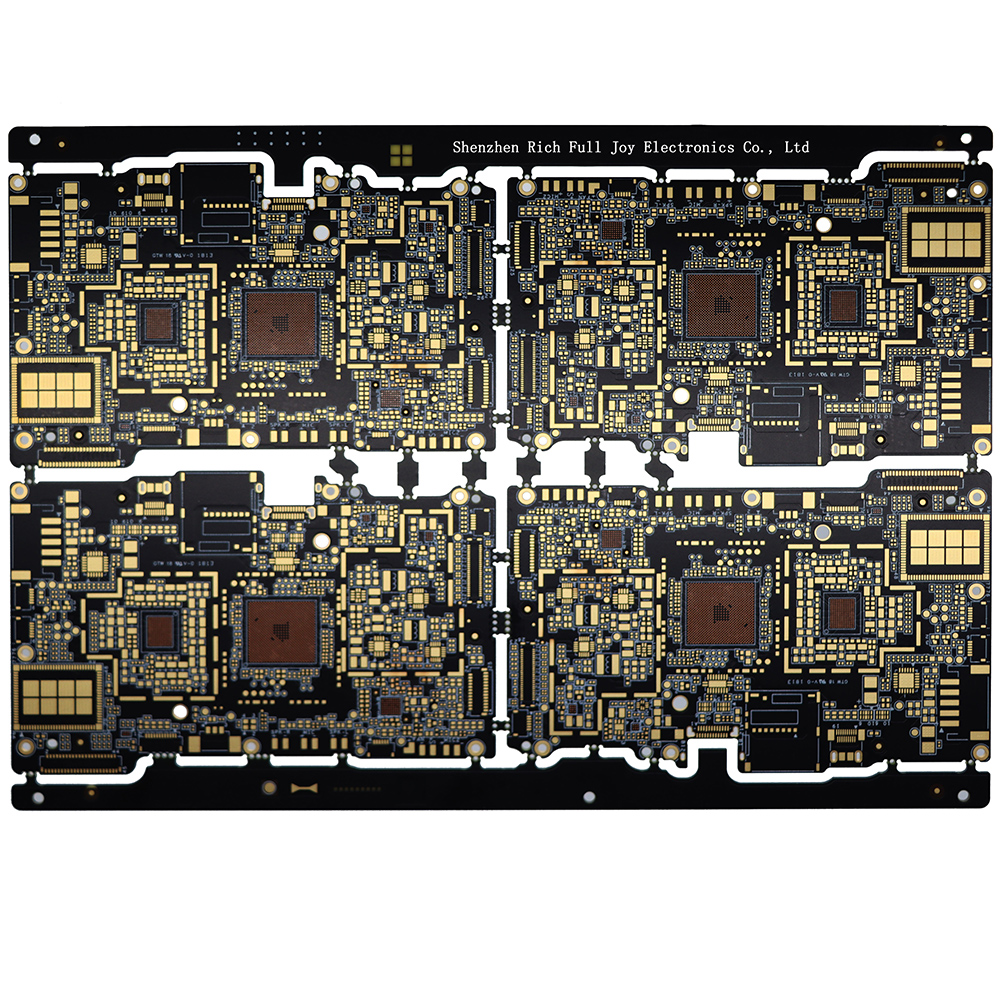


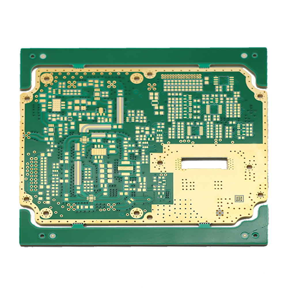
Any Layer High Density Interconnected PCB


BASIC CONCEPT OF HDI

HDI stands for High Density Interconnector, which is a PCB manufacturing type (technology), using micro blind/buried via technology to realize a high line distribution density. It can achieve smaller dimensions, higher performance and lower costs. HDI PCB is the pursuit of designers, constantly developing towards high density and precision. The so called “high” not only improves machine performance, but also reduces machine size. High Density Integration (HDI) technology can make end product design more miniaturized, while meeting higher standards of electronic performance and efficiency.
HDI PCB typically includes laser drilling blind via and mechanical drilling blind via. The technology of conducting between inner and outer layers is generally achieved through processes such as through buried via, blind via, stacked holes, staggered holes, cross blind/buried via, through holes, blind via filling electroplating, fine wire small space and micro holes in the disc, etc.
There’re several types of HDI PCB : 1 layer, 2 layer, 3layer, 4 layer and any layer interconnection.
● Structure of 1 layer HDI : 1+N+1 (pressing twice, laser drilling once).
● Structure of 2 layer HDI : 2+N+2 (pressing 3 times, laser drilling twice).
● Structure of 3 layer HDI : 3+N+3 (pressing 4 times, laser drilling 3 times).
● Structure of 4 layer HDI : 4+N+4 (pressing 5 times, laser drilling 4 times).
From the above structures, it can be concluded that laser drilling once is a 1 layer HDI, twice is a 2 layer HDI, and so on. Any layer Interconnection can start laser drilling from the core board. In the other word, what needs to be laser drilled before pressing is any layer HDI.
Design Concept of HDI
1.When we encounter a design with holes in the BGA area of a multi-layer PCB, but due to space constraints, we have to use ultra small BGA pads and ultra small holes to achieve full board penetration, how should we make it? Now we’d like to introduce the HDI high precision PCB mentioned frequently in PCBs as following.
The traditional drilling of PCB is affected by the drilling tool. When the drilling hole size reaches 0.15mm, the cost is already very high and it is difficult to improve more. However, due to limited space, when only a 0.1mm hole size can be adopted, the design concept of HDI is needed.
2. The drilling of HDI PCB no longer relies on traditional mechanical drilling, but utilizes laser drilling technology (sometimes also known as laser board). The drilling hole size of HDI is generally 3-5mil (0.076-0.127mm), the line width is 3-4mil (0.076-0.10mm), the size of solder pads can be greatly reduced, so more line distribution can be obtained per unit area, resulting in high density interconnection.

The emergence of HDI technology has adapted to and promoted the development of PCB industry, enabling more dense BGA, QFP, etc. to be arranged on the HDI PCB. Presently, HDI technology has been widely used, among which 1 layer HDI has been widely used in the PCB production with 0.5pitch BGA. The development of HDI technology is driving the development of chip technology, which in turn drives the improvement and progress of HDI technology.
Nowaday 0.5pitch BGA chips have gradually been widely adopted by design engineers, and the solder joints of BGA have gradually changed from a center hollowed out or grounded form to a form with signal input and output at the center that requires wiring.
3. HDI PCB is generally manufactured using stacking method. The more times the stacking is done, the higher the technical level of the board. Ordinary HDI PCB is basically stacked once, while high layer HDI uses two times or more stacking technology, as well as advanced PCB technologies such as hole stacking, hole filling by electroplating and direct laser drilling, etc.
HDI PCB is conducive to the use of advanced assembly technology, and the electrical performance and signal accuracy are higher than traditional PCB. In addition. HDI has better improvements in radio frequency interference, electromagnetic wave interference, electrostatic discharge and thermal conduction, etc.
Application

HDI PCB has a wide range of application scenarios in the electronic field, such as :
-Big Data & AI : HDI PCB can improve the signal quality, battery life and functional integration o mobile phones, while reducing their weight and thickness. HDI PCB can also support the development of new technologies such as 5G communication, AI and IoT, etc.
-Automobile : HDI PCB can meet the complexity and reliability requirements of automotive electronic systems, while improving the safety, comfort and intelligence of automobiles. It can also be applied to functions such as automotive radar, navigation, entertainment and driving assistance.
-Medical : HDI PCB can improve the accuracy, sensitivity and stability of medical equipments, while reducing their size and power consumption. It can also be applied in fields such as medical imaging, monitoring, diagnosis and treatment.
The mainstream applications of HDI PCB are in mobile phones, digital cameras, AI, IC carriers, laptops, automotive electronics, robots, drones, etc., being widely used in multiple fields.
