


01

Multilayer PCB, any layer HDI PCB


High layer/any layer HDI manufacturer

The definition of HDI (High Density lnterconnection) circuit board refers to a Microvia PCB with an aperture of less than 6mm, a Hole Pad of less than 0.25mm, a contact density of more than 130 points/square hour, a wiring density of more than 117 points/square hour, and a line width/spacing of less than 3mi/3mi.
Classification of HDI PCB : 1 layer, 2 layer, 3 layer and any layer HDI
1 layer HDI structure : 1+N+1 (press twice, laser once).
2 layer HDI structure : 2+N+2 (press 3 times, laser twice).
3 layer HDI structure : 3+N+3 (press 4 times, laser 3 times).
Any layer HDI refers to the HDI that can process the laser drilling from the core PCB, in the other word, it means that the laser drilling is required before pressing.
The advantages of HDI PCB
1. It can reduce PCB costs. When the PCB density increases to more than 8 layers, it is manufactured in the way of HDI and its cost will be lower than traditional complex pressing processes.
2. Increase circuit density by interconnecting traditional circuit boards and components
3. Beneficial for the use of advanced packaging technology
4. Possess better electrical performance and signal accuracy
5. Better reliability
6. Can improve thermal performance
7. Can reduce radio frequency interference, electromagnetic wave interference, and electrostatic discharge (RFI/EMI/ESD)
8. Increase design efficiency

The main differences between HDI and regular PCB
1. HDI has a smaller volume and lighter weight
HDI PCB is made of traditional double-sided PCB as the core, through continuous build-up and lamination. This type of circuit board made by continuous layering is also known as Build-up Multilayer (BUM). Compared to traditional circuit boards, HDI circuit boards have advantages such as being light, thin, short and small.
The electrical interconnection between HDI circuit boards is achieved through conductive through-hole, buried/blind via connections, which are structurally different from ordinary multi-layer circuit boards. Micro buried/blind via is widely used in HDI PCBs. HDI uses direct laser drilling, while standard PCBs usually use mechanical drilling, so the number of layers and aspect ratio often decrease.
2. Manufacturing Process of HDI main board
The high-density development of HDI PCBs is mainly reflected in the density of holes, circuits, solder pads and interlayer thickness.
● Micro through-holes: HDI PCBs contain blind holes and other micro through-hole designs, which are mainly manifested in the high requirements of micro hole forming technology with a pore size less than 150um, as well as cost, production efficiency and hole position accuracy control. In traditional multi-layer circuit boards, there are only through-holes and no small buried/blind holes
● Refinement of line width/spacing: mainly manifested in increasingly strict requirements for wire defects and wire surface roughness. The general line width/spacing do not exceed 76.2um
● High pad density: The density of solder joints is greater than 50/cm2
● Thinning of dielectric thickness: This is mainly manifested in the trend of interlayer dielectric thickness developing towards 80um and below, and the requirement for thickness uniformity is becoming increasingly strict, especially for high-density PCBs and packaging substrates with characteristic impedance control
3. HDI PCB has better electrical performance
HDI can not only miniaturize end product design, but also meet higher standards of electronic performance and efficiency simultaneously.
The increased interconnect density of HDI allows for enhanced signal strength and improved reliability. In addition, HDI PCBs have better improvements in reduction of radio frequency interference, electromagnetic wave interference, electrostatic discharge and heat conduction, etc. HDI also adopts fully digital signal process control (DSP) technology and multiple patented technologies, which have the ability to adapt to loads in a full range and strong short-term overload capacity.
4. HDI PCBs have very high requirements for buried via/plug hole
As can be seen from the above, both in terms of board size and electrical performance, HDI is superior to ordinary PCBs. Every coin has two sides, and the other side of HDI, as a high-end PCB, its manufacturing threshold and process difficulty are much higher than ordinary PCBs, and there are also many issues to pay attention to during production, especially the buried via and plug hole.
At present, the core pain point and difficulty in HDI production and manufacturing is the buried via and plug hole. If the HDI buried via / plug hole is not done well, significant quality problems will occur, including uneven edges, uneven medium thickness and potholes on the solder pad.
● Uneven board surface and uneven lines can cause beach phenomena in sunken areas, leading to defects such as line gaps and breaks
● The characteristic impedance may also fluctuate due to uneven dielectric thickness, causing signal instability
● Uneven solder pads result in poor subsequent packaging quality, leading to joint and several losses of components
Therefore, not all PCB factories have the ability and strength to do HDI well, and RICH PCBA has been working hard for this over 20 years.
We have achieved good results in special designs such as high-precision, high-density, high-frequency, high-speed, high TG, carrier plates and R-F PCB. We also have rich producing experience in special processes such as ultra-thick, oversized, thick copper, high-frequency hybrid pressure, copper inlaid blocks, half holes, back drills, depth-control drills, gold fingers, high-precision impedance control boards, etc.
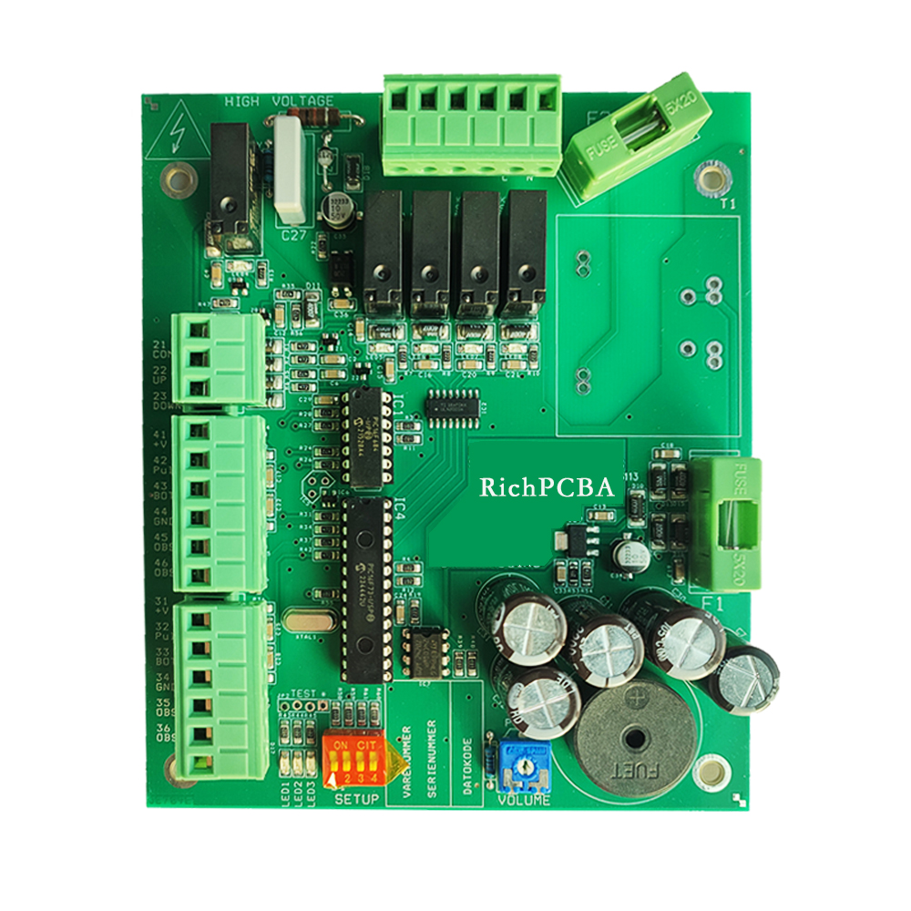
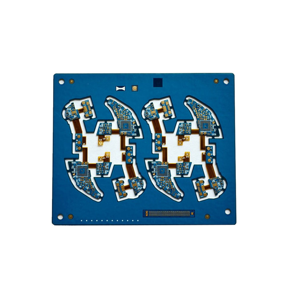
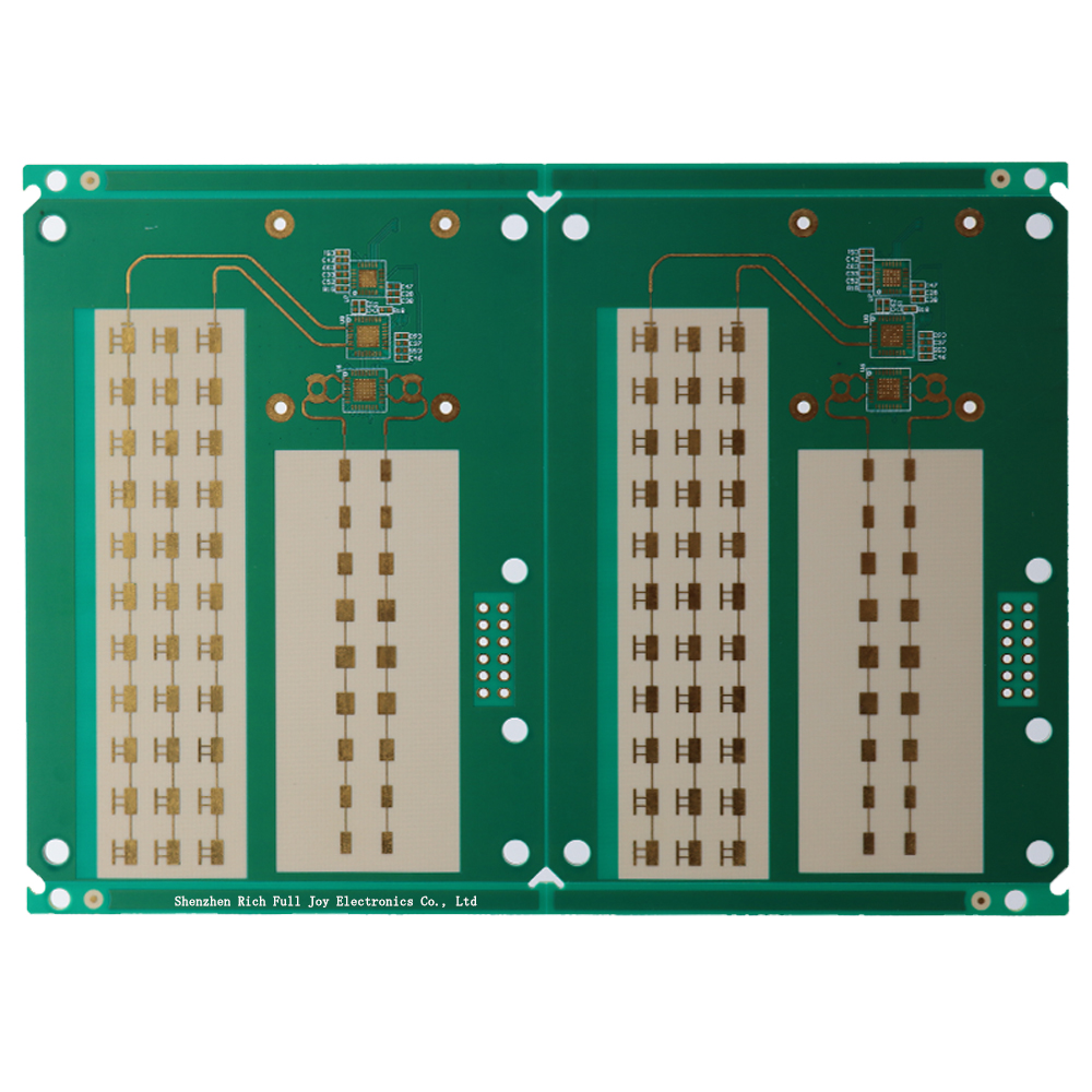
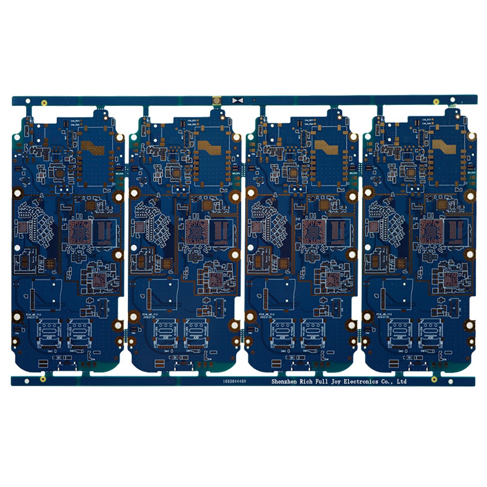
Application (see attached figure for details)
HDI PCBs are used in a wide range of fields such as mobile phones, digital cameras, AI, IC carriers, medical equipment, industrial control, laptops, automotive electronics, robots, drones, etc.

Application
HDI PCBs are used in a wide range of fields such as mobile phones, digital cameras, AI, IC carriers, medical equipment, industrial control, laptops, automotive electronics, robots, drones, etc.