Leave Your Message
-
E-mail
-
Whatsapp
-
Message
With the growing needs of new-age electronic devices, High Frequency PCBs have become an immense and significant part of technology today. These state-of-the-art printed circuit boards are highly beneficial to the applications where efficient signal transmission occurs and loss is minimized-their applications take place in telecommunications, aerospace, and automotive sectors, among others. With technology evolving fast, trends in the global market are increasingly relevant to understanding how High Frequency PCB technology will also take shape and develop in future applications.
At the company, Shenzhen Ruizhi Xinfeng Electronics Co., Ltd, we are at the forefront of this transformation, accompanying high-quality custom-made printed circuit solutions that meet the rigorous demands of today's markets. Understanding future trends in High Frequency PCB technology will not only help enhance our products but will also help our clients make safer and informed decisions on what to buy. Going through the future emerging developments and progressive advancements in this field clearly indicates that this is the strategy to stay ahead of trends in the highly competitive arena.
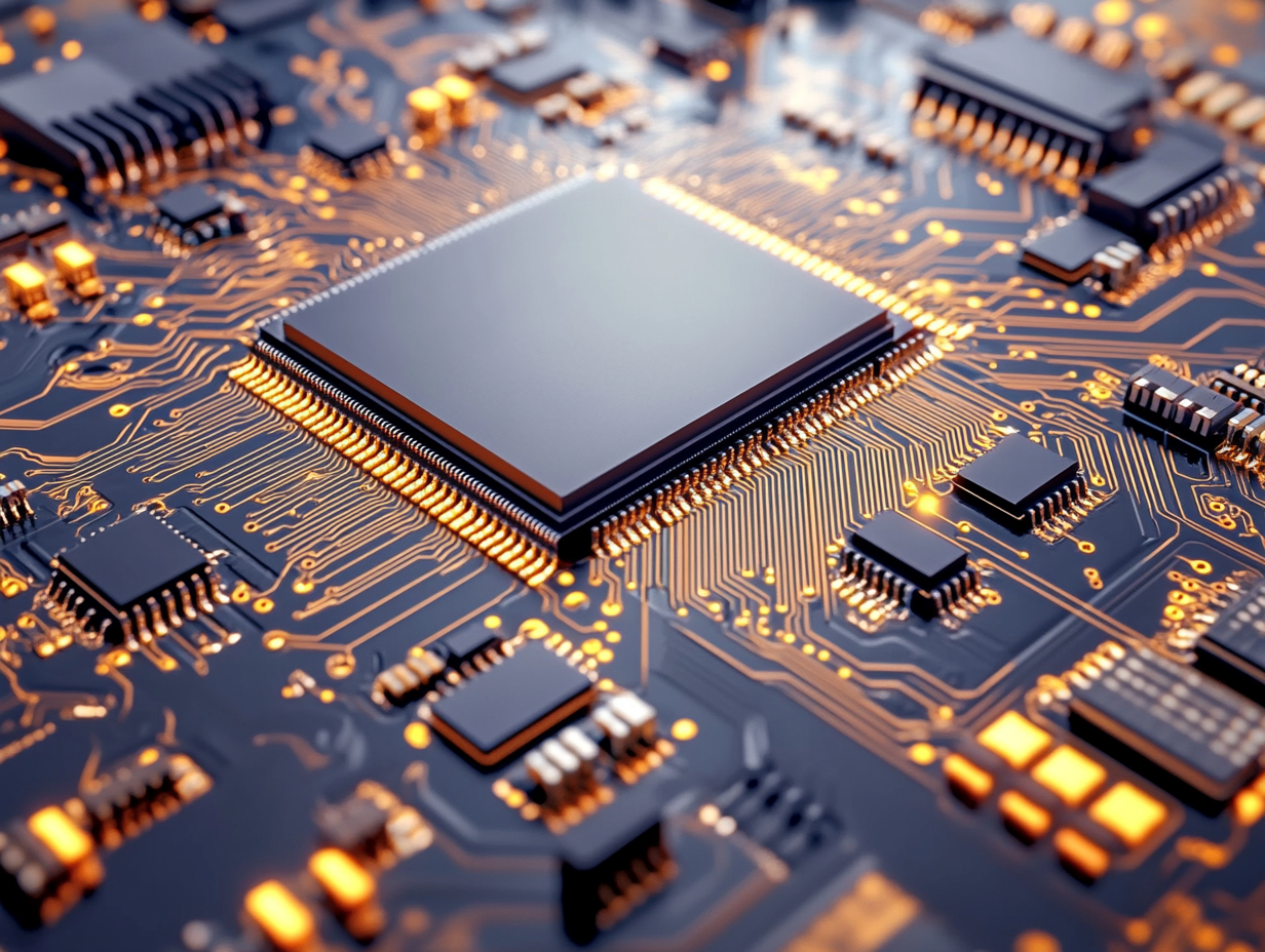
Without a doubt, the core technology involved in high-frequency printed circuit boards (PCBs) lies somewhere within the aerospace and telecommunications applications. As the world moves towards much faster and highly reliable electronic devices, so does the direction that high-frequency PCBs take in this development. These tend to be PCBs built to handle the higher signals with lower losses in interconnection-the main effects in developing more efficient amplifiers and integrated circuits that can be offered commercially and for military applications. New semiconductor technologies coupled with novel collaborations within the industry all herald a great step toward the implementation of high-frequency PCBs. Examples include a number of the latest-generation power amplifiers, which are now being integrated towards everyday products as high frequency becomes mainstream in consumer access. Trends like this are ever so vital for understanding how global buyers might remain competitive in an evolving marketplace as manufacturers strive to satisfy these emerging demands.

So, now that the demand for high frequency is becoming consolidated into an imperative, so are the considerations for sustainable production processes. Manufacturers are now concentrating on environmentally friendly materials and manufacturing processes that are waste minimizing and energy efficient. In this way, they would be continuing to meet regulatory requirements but also satisfying the needs of eco-aware consumers.
The semiconductor technology of recent years, with gallium nitride (GaN) amplifiers entering the picture, is the best example applicable to sustainable practices. These innovations lead often collaboratively to designs that are small, lightweight, and hence much more efficient, contributing to lower energy consumption by electronic devices in the aggregate. With rendezvous like these to eco-friendly trends, the high-frequency PCB sector could do a lot to bolster its role in the worldwide effort toward sustainability while evolving even further in performance to meet commercial and military needs.

Recent technological advances, especially those in communication like 5G and the next 6G, are pushing new applications in high-frequency PCBs to the forefront. With networks going towards ultra-high-speed connectivity, innovative designs for PCBs will gain higher importance. High-frequency PCBs have, therefore, become the very life & breath of performance and reliability for several gadgets ranging from mobile phones to sophisticated radar systems.
Integration of the millimeter-wave technology into consumer goods is now changing marketplace needs. PCB designers are therefore finding their role rapidly evolving as manufacturers are employing ever-more-complex designs to support even more enhanced functionalities. In the foreseeable future, there will possibly be more emphasis on electro-optical circuit boards with a view to maximizing data-transmission capabilities against the backdrop of an ever-increasing need for compactness and efficiency. These trends create a promising horizon for global buyers in the printed circuit board market and innovation on groundbreaking applications.

With the coming of the year 2031, the world market for high frequency PCBs is said to take a broad leap. Recent studies have shown what would be groundbreaking trends-increasing demand in telecommunications, aerospace, and medical devices-powered by the next generation technology. As industries apply high-frequency transmission further for performance and efficiency, manufacturers adapt by innovating their PCB designs and materials.
This calls for developing collaborations and product introductions that provide the foundation for both availability and tech capabilities in high-frequency PCBs. One of these strategic partnerships is within the semiconductor industry to enhance an application value proposition in high-frequency applications. The market shows signs of definite trends, moving towards even more sophisticated designs that leverage advanced materials, all going with the aim to satisfy the new global buyers increasingly looking for reliable and efficient circuit board solutions.
The global demand for high-frequency PCBs increases, meaning buyers have to rethink their sourcing strategies to take advantage of changing technologies. The recent movement toward mmWave application, which previously would not have been considered apart from military or satellite realms, is an example of a rapidly evolving scenario. Such a shift witnesses an increased emphasis placed on sourcing materials able to tackle 5G and future challenges, which are in many cases high-frequency and complex antenna packaging requirements.
Global buyers who would like to stay competitive should fall keenly within the arena of trends in copper clad laminates-a market set to see significant growth in coming years. Furthermore, keeping a watchful eye on the developments in Antenna in Package (AiP) technologies will be paramount since these very developments drive PCB designs and functionalities. By synchronizing their sourcing strategies with these emerging trends, buyers will arguably be able to meet future expectations in the high-frequency PCB market.
The emergence of new high-performance applications is dramatically transforming the future of high-frequency PCBs. The advanced copper clad laminates are some of the key materials that play this transformation role, as the market for these kinds of laminates is sharply expected to grow, soaring to an estimated USD 16.40 billion by 2030. The booming markets for 5G, Internet of Things (IoT), and radar technologies are driving this upsurge as all these applications require robust and yet highly reliable PCB materials.
Furthermore, antenna packaging innovation is equally that critical consideration for future high-frequency PCBs. Millimeter-wave applications are now destined for the public arena, extending beyond military and automotive applications into mobile technologies. With that integration, the newer materials must be introduced to minimize the attenuation of signals. The AI-enabled cognitive radio systems are destined to connect better than before, and all of this occurrence opens new opportunities for further high-frequency PCB application in telecommunications as it advances.
The importance of high-frequency PCBs nowadays cannot be stressed enough, as they are solid components in modern electronics. They are said to support high data transmission rates that are just perfect for upcoming technologies like 5G and the supposed 6G. Connects more devices at increased speeds, and as a result, high-frequency boards become part of telecommunications, automotive, and IoT, among many other sectors.
Additionally, advances in materials and processes have improved performance of high-frequency PCBs so that signal integrity improves and attenuation reduces. Such improvements in performance become more crucial for applications using millimeter-wave frequencies that have gradually been transformed from niche applications to mainstream consumer electronics. As such, the expanding need for global buyers to obtain cutting-edge solutions makes high-frequency PCB technology continuosly evolve, thereby transforming innovation in multiple electronic platform.
High-frequency PCB technology in particular is fast evolving and has much application in various fields such as telecommunications and defense. In addition, the growth of advanced components, including high-performance GaN power amplifiers, would further improve efficiency and other applications. Research on bettering material properties and also focusing on signal integrity in PCB designs will come as demands in the market grow and will begin to deal with increased miniaturization, which does not compromise functionality.
Future research directions in high-frequency PCB technology could investigate the use of cost-effective, efficient manufacture methods that considerably shorten production time. Simulation software advances might make performance prediction easier than high-frequency conditions. As globally, the printed circuit boards business is growing significantly up to 2031; thus, required will be more advanced research and development in line with industry standards and comparative advantages. The collaboration between component manufacturers and PCB producers will play a pivotal role in driving these innovations forward.
Manufacturing techniques of high-frequency PCBs possess numerous challenges that the industry should address. One of the major problems included is in materials, since the traditionally used substrates usually do not fulfill the performance specifications required for high-frequency applications. The increasing demand is therefore urging manufacturers to innovate newer materials that possess better electromagnetic properties.
Furthermore, precision in fabrication becomes critical. The production process is required to maintain very high accuracy to ensure minimal signal loss and interference during the manufacturing and application stages for high-frequency PCBs. The complicated nature of such PCBs translates to increasing production costs and availability of skilled manpower and advanced manufacturing technologies. Thus it is becoming necessary to address these challenging manufacturing issues in order to serve the changing demands of the global electronics market, which increasingly wants high efficiency and reliability.
With 5G technology and IoT fast coming into play, demand for high-frequency PCBs is gaining momentum. While the technologies transition to mainstream application, advanced PCBs that can withstand higher frequencies and greater data throughput are becoming an absolute necessity. Consequently, manufacturers are being compelled to innovate and change materials and designs in order to meet the requirements for high-speed communication.
With a rapid growth forecast for the global PCB market, companies are investing in advanced technology to support the growing needs of industries including telecommunications and military applications. Recent partnerships and product introductions in the semiconductor market bear testimony to the continuing trend that is placing an additional burden on high-frequency PCBs in meeting the performance demands from 5G and IoT devices. Looking forward, global buyers will find it imperative to keep a step ahead of these trends to secure the most effective solutions for their electronic needs.
High-frequency PCBs are circuit boards designed to operate efficiently at high frequencies, crucial for applications like telecommunications and 5G technology. Their demand is rising due to the increasing adoption of mmWave applications and the need for advanced communication technologies.
The shift towards mmWave applications emphasizes the need for sourcing materials that support high-frequency capabilities and sophisticated antenna packaging, necessitating an adaptation in sourcing strategies for global buyers.
It is critical for buyers to understand trends in the copper clad laminates market, as it is projected to grow significantly, impacting the sourcing decisions for high-frequency PCBs.
AiP technologies influence PCB design and functionality significantly; staying informed about these advancements is essential for buyers to align their sourcing with future market demands.
Future research may focus on improving material properties, enhancing signal integrity, exploring innovative manufacturing methods, and advancing simulation software for performance predictions under high-frequency conditions.
GaN power amplifiers are expected to enhance efficiency and performance in high-frequency PCB applications, driving further advancements in the technology.
Collaboration is crucial as it fosters innovation and drives improvements in high-frequency PCB technology, helping both parties to meet market demands and industry standards.
High-frequency PCBs require advanced designs that ensure signal integrity and performance, posing challenges in material selection, manufacturing processes, and ensuring miniaturization without functionality loss.
The global market for printed circuit boards is projected to expand significantly by 2031, necessitating cutting-edge research and development to meet evolving industry standards.
Effective sourcing strategies are essential for global buyers to ensure they can meet the future demands of the high-frequency PCB market and remain competitive in an evolving technological landscape.