Leave Your Message
-
E-mail
-
Whatsapp
-
Message
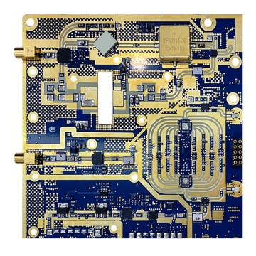
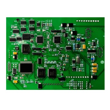
Precision-engineered PCB and PCBA products purpose-built for automotive camera systems integrated within modern electric vehicle charging environments.
The rapid global expansion of electric vehicle (EV) charging infrastructure has created an unprecedented demand for intelligent, reliable, and high-performance electronic systems embedded within charging stations, parking facilities, and smart grid nodes. At the heart of this transformation lies the Car Camera PCB — a specialized printed circuit board engineered to support automotive-grade camera modules deployed across charging environments for purposes ranging from vehicle identification and safety monitoring to automated payment and AI-driven diagnostics.
📡 Key Insight: By 2030, the global EV charging infrastructure market is projected to exceed $100 billion. Car Camera PCBs are becoming a mission-critical component enabling smart, automated, and secure charging ecosystems worldwide.
Modern EV charging stations are no longer simple power dispensers — they are intelligent nodes within a connected urban mobility network. Cameras integrated into these stations perform license plate recognition (LPR), occupancy detection, fraud prevention, driver assistance, and real-time video analytics. All of these functions require PCBs that can handle high-frequency signal processing, thermal management, and multi-layer data routing in compact, ruggedized form factors.
Shenzhen Rich Full Joy Electronics Co., Ltd. has positioned itself at the forefront of this convergence, delivering custom Car Camera PCB and PCBA solutions that meet the stringent demands of automotive and industrial charging infrastructure clients globally. With 20 years of manufacturing expertise and certifications including IATF16949 and ISO9001, the company provides end-to-end solutions from PCB design to full assembly and testing.
Why Car Camera PCBs for charging infrastructure demand the most advanced manufacturing processes
Camera image data streams require PCBs with controlled impedance traces, low-loss dielectrics, and minimal EMI — especially critical in high-voltage EV charging environments where electromagnetic interference is significant.
Charging stations operate in outdoor environments with extreme temperature ranges. Car Camera PCBs must incorporate advanced thermal vias, copper pours, and heat-dissipating substrates to maintain image processor stability.
Compliance with IATF16949 and AEC-Q100 standards ensures that every PCB delivered for charging infrastructure camera systems meets the reliability benchmarks of the automotive supply chain — no compromises.
High-Density Interconnect (HDI) technology enables the miniaturization of camera processing boards while increasing routing density — essential for compact charging station enclosures with limited PCB real estate.
AI-powered camera modules running real-time object detection algorithms demand clean, stable power delivery. Advanced power plane design and decoupling strategies ensure noise-free operation even during rapid charge cycles.
Modern charging cameras transmit data via 4G/5G, Wi-Fi 6, or wired Ethernet. PCBs must support RF antenna integration, shielding, and multi-protocol communication interfaces within a single compact board design.
Understanding where Car Camera PCBs fit within today's EV charging infrastructure ecosystem
As of 2024, there are over 3 million public EV charging points globally, with projections indicating this number will surpass 40 million by 2030. Major charging network operators — including ChargePoint, EVgo, Shell Recharge, and IONITY — are actively deploying camera-equipped stations to enhance user experience, reduce fraud, and enable fully automated, contactless charging sessions. This commercial momentum has created a thriving B2B market for high-quality Car Camera PCB assemblies.
The industrial segment is equally compelling. Logistics depots, fleet management centers, and commercial parking structures are integrating camera-enabled charging bays that can automatically identify vehicles, initiate charging sessions, and log usage data — all without human intervention. These systems rely on ruggedized PCBs capable of continuous 24/7 operation in demanding industrial environments.
Global supply chain disruptions have accelerated the trend toward vertically integrated PCB manufacturers that can offer design, fabrication, and assembly under one roof. Charging infrastructure OEMs increasingly prefer partners like Rich Full Joy Electronics, who can deliver from Gerber files to fully tested PCBA boards, reducing lead times and minimizing quality risks across the supply chain.
The shift toward domestically produced, high-reliability PCBs is particularly pronounced in North America and Europe, where government incentives for EV infrastructure are tied to local content requirements. Chinese manufacturers with international certifications and proven automotive-grade processes are well-positioned to serve these markets as trusted global suppliers.
Next-generation camera PCBs are integrating edge AI chips (NPUs) directly onto the board, enabling real-time inference for license plate recognition, vehicle classification, and anomaly detection — eliminating latency from cloud-dependent architectures.
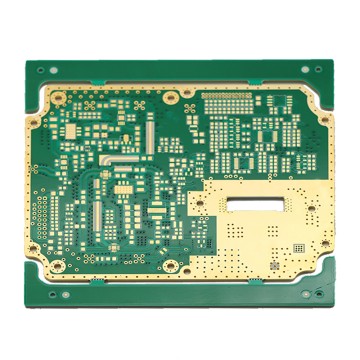
As charging stations become 5G-connected smart infrastructure nodes, camera PCBs must integrate multi-band RF front-ends, MIMO antenna arrays, and advanced EMC shielding — demanding new high-frequency hybrid PCB materials and processes.
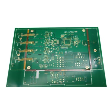
Space constraints in modern charging station designs are driving adoption of rigid-flex PCB technology, allowing camera modules to be mechanically integrated into curved or irregular enclosure geometries without sacrificing signal integrity.
Outdoor charging cameras must operate from -40°C to +85°C. PCB material selection, conformal coating processes, and specialized surface finishes are evolving to meet increasingly stringent environmental protection requirements.
Vehicle-to-Grid (V2G) technology requires cameras to identify not just the vehicle but also its battery state and grid interaction status. PCBs must now support bidirectional data interfaces and advanced power monitoring ICs within the same assembly.
With charging infrastructure classified as critical national infrastructure in many countries, camera PCBs are increasingly required to incorporate hardware security modules (HSM), secure boot chips, and encrypted communication interfaces at the board level.
How Car Camera PCBs are deployed across diverse charging infrastructure environments
High-traffic city charging plazas deploy camera PCBs for automatic bay allocation, real-time occupancy monitoring, and contactless user authentication via license plate or QR code recognition — reducing queue times and maximizing station utilization rates.
Logistics companies operating large EV fleets require automated charging management. Camera PCBs enable vehicle identification upon arrival, automatic charging slot assignment, and integration with fleet management software for billing and maintenance scheduling.
Integrated parking-charging facilities use camera PCBs to manage both parking access control and EV charging simultaneously. A single camera node handles entry/exit recognition, charging initiation, and payment processing through a unified PCB platform.
High-speed highway charging stations demand ultra-reliable camera systems for safety monitoring and incident detection. PCBs in these environments must withstand extreme vibration, temperature cycling, and continuous high-duty-cycle operation.
Corporate campuses and commercial buildings integrate camera-enabled charging with employee access control systems. PCBs support facial recognition or RFID-linked vehicle identification, enabling seamless employee benefit management and energy cost allocation.
Electrification of port equipment and heavy-duty trucks requires industrial-grade camera PCBs that can operate in harsh maritime environments with high humidity, salt spray, and extreme load cycles — necessitating military-spec conformal coating and ruggedized connector interfaces.
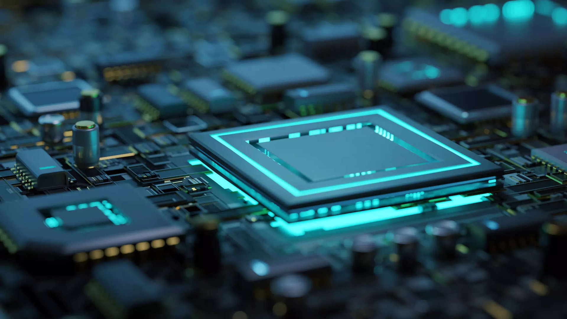
Based in China and looking at the global market, Shenzhen Rich Full Joy Electronics Co., Ltd. has been committed to industry development for 20 years. The company is a national high-tech innovative enterprise that combines focus and expertise. It's also an important enterprise incubation base in China. We specialize in providing customers with one-stop intelligent electronic manufacturing services, including scientific research, PCB design, PCB manufacturing, PCB assembly (including SMT, DIP, Programming and testing) and component selection.
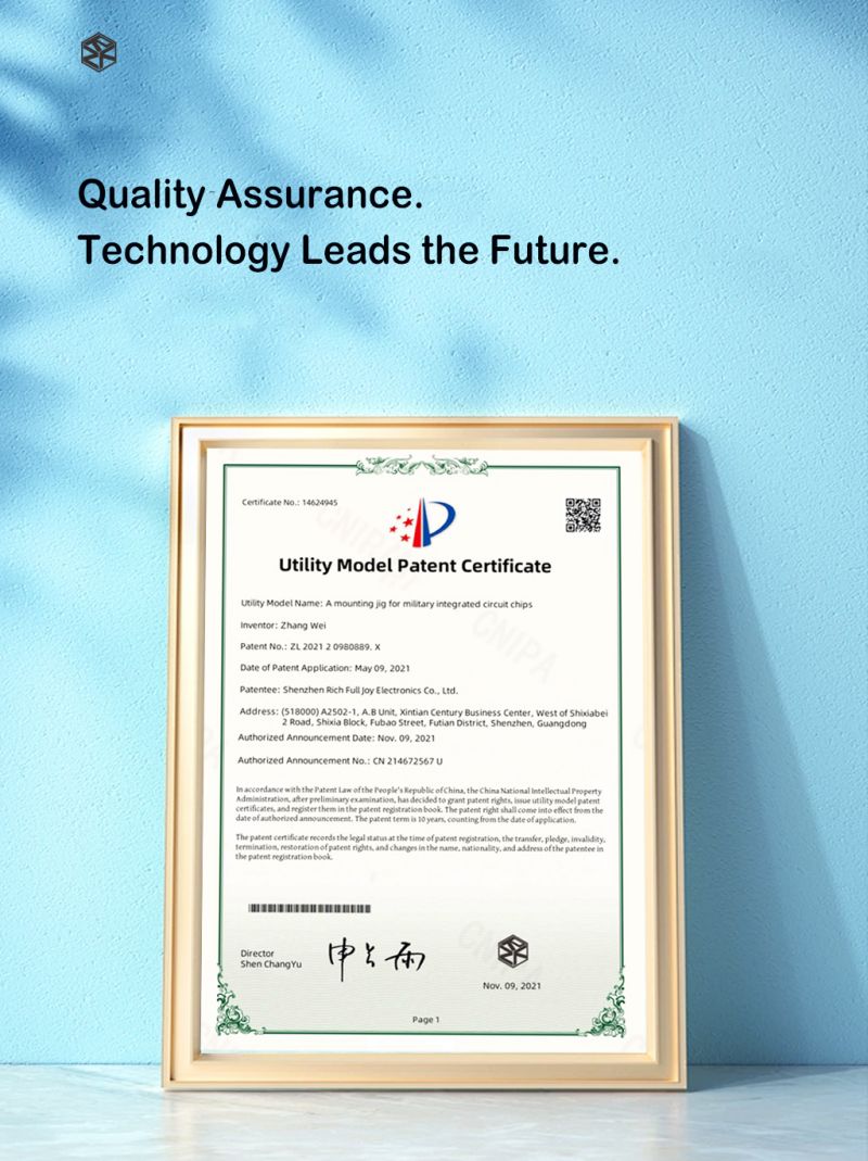
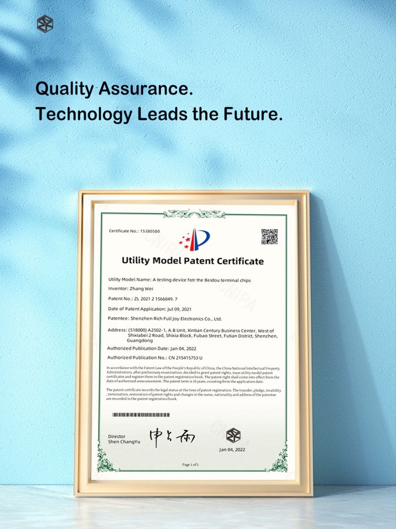
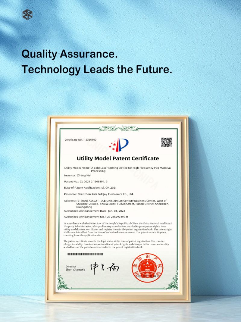
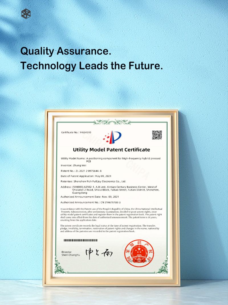
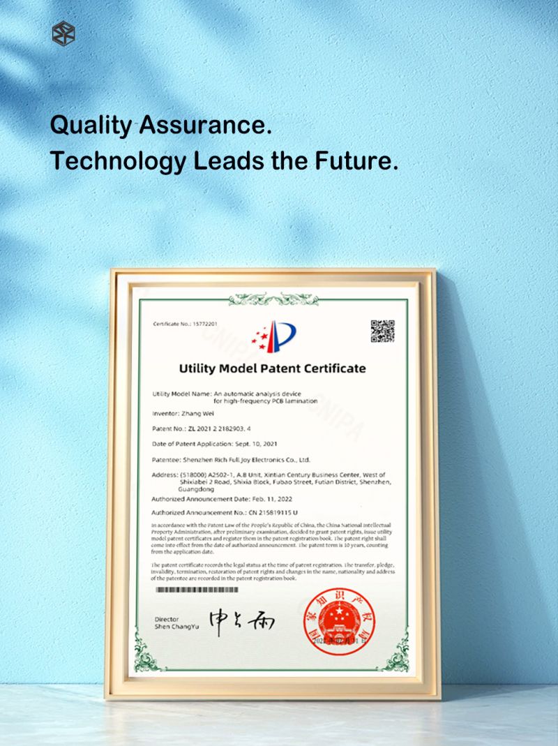
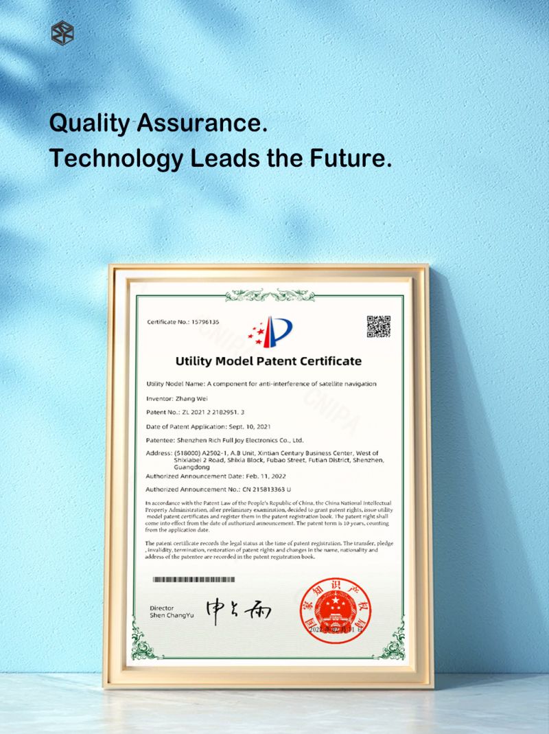
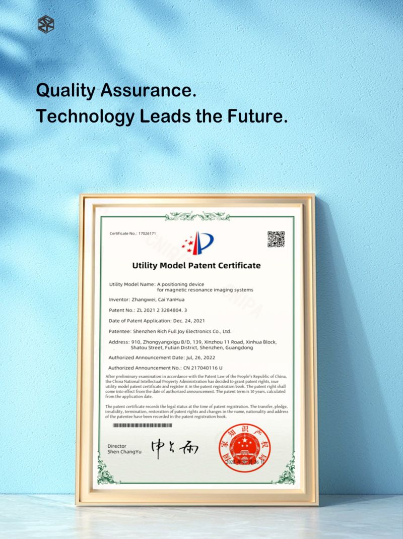
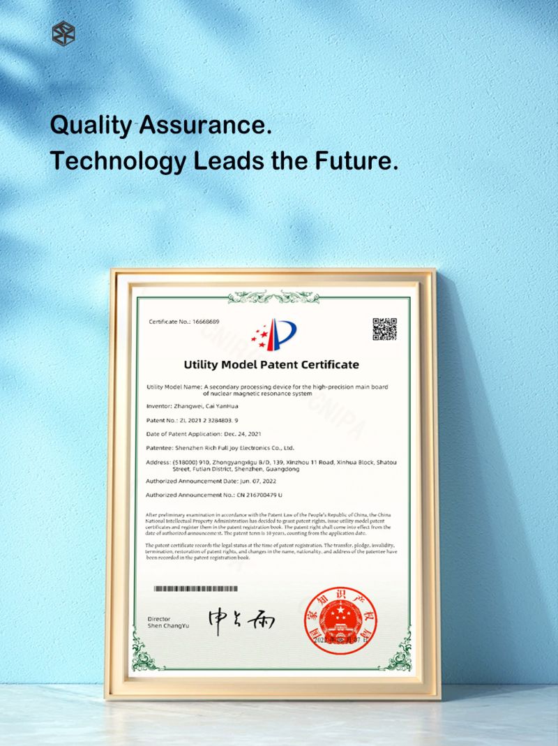
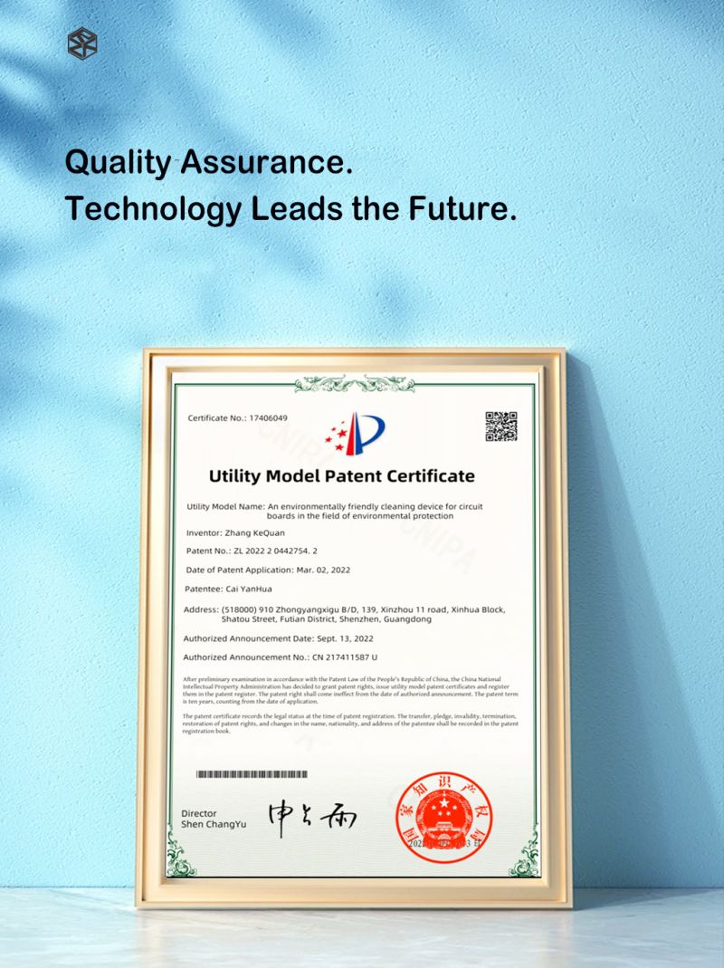
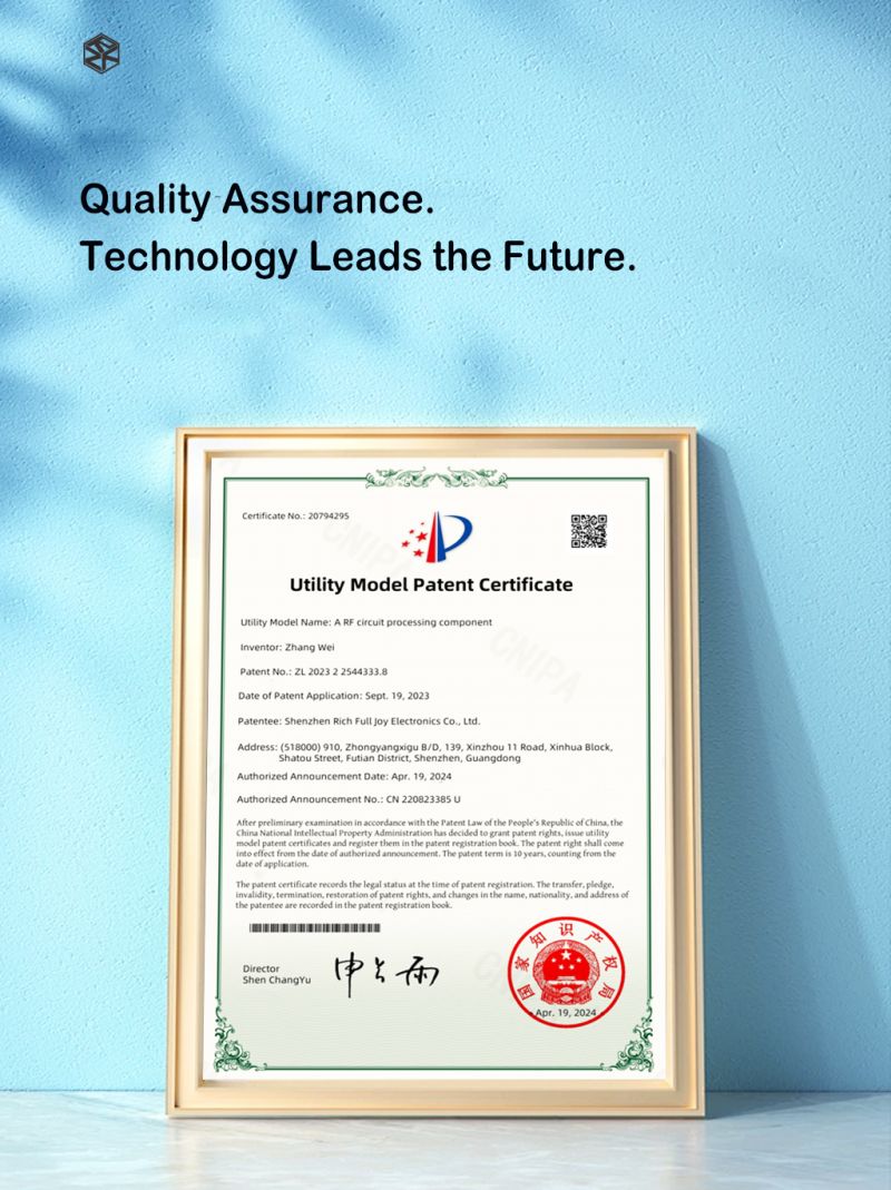
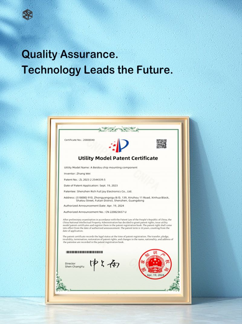
Technological innovation is the core competitiveness of our enterprise. We've obtained multiple invention and utility model patents, and have passed various international standard certifications such as ISO9001, IATF16949, ISO14001, UL, CQC, REACH, RoHS, COC, as well as the GJB9001C-2017 standard certification for weapon and equipment quality management system. We've provided high-quality and reliable products to multiple research institutions, universities, and assisted customers in identifying design issues and providing reasonable suggestions and processing parameters.
We not only publish technical papers, but also actively participate in domestic and overseas technology exchange conferences to spread academic value and cutting-edge technological innovation. We regularly communicate with customers and strive to provide them with the best solutions for every application — including Car Camera PCBs for next-generation charging infrastructure.
Our intellectual property portfolio and international certifications underpin every Car Camera PCB we manufacture for charging infrastructure clients











Explore our full range of PCB and PCBA products engineered for automotive camera and EV charging applications