Leave Your Message
-
E-mail
-
Whatsapp
-
Message
From high-frequency RF boards to HDI multilayer designs, our PCB products are purpose-built for demanding EV powertrain and charging station environments.
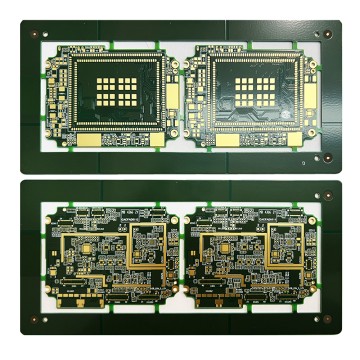
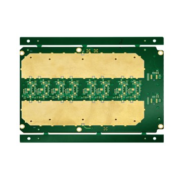
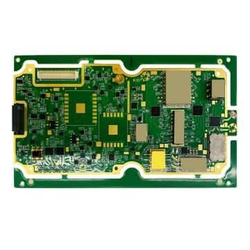
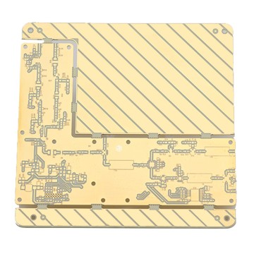
The global transition to electric mobility is accelerating at an unprecedented pace. At the heart of every electric vehicle charging station — from compact Level 2 AC wall boxes to ultra-fast 350 kW DC fast chargers — lies a sophisticated array of printed circuit boards (PCBs). The Charging Station PCB for EV Powertrain is not merely a passive substrate; it is the intelligent nervous system that governs power conversion, energy management, thermal protection, communication, and safety compliance across the entire charging ecosystem.
As EV adoption surges globally, demand for high-performance, thermally robust, and electromagnetically resilient PCBs has skyrocketed. Engineers and procurement specialists are now scrutinizing board-level design with the same rigor applied to battery chemistry and motor control algorithms. The performance ceiling of an EV charging station is, in many cases, defined by the quality of its PCB design and manufacturing.
A single thermal runaway event on an improperly designed power stage PCB can destroy a $50,000 DC fast charger. Precision impedance control, advanced via-in-pad technology, and high-Tg laminate selection are not optional — they are engineering imperatives for any charging station PCB deployed in real-world EV powertrain environments.
The EV charging infrastructure market was valued at over USD 28 billion in 2023 and is projected to exceed USD 220 billion by 2032, growing at a CAGR above 25%. This explosive growth is directly translating into massive demand for specialized PCBs capable of operating reliably under high-voltage, high-current, and high-frequency switching conditions.
Commercially, the market is bifurcated into two primary segments: residential and commercial AC charging (Level 1 & Level 2) and public DC fast charging (Level 3). Each segment imposes distinct PCB design requirements:
Several macro-trends are reshaping how charging station PCBs are designed, specified, and manufactured:
The adoption of Silicon Carbide (SiC) MOSFETs and Gallium Nitride (GaN) transistors in power stages is forcing PCB designers to handle switching frequencies above 100 kHz with minimal parasitic inductance. This demands ultra-tight impedance control, blind/buried via structures, and advanced copper fill strategies in the PCB stack-up.
As charger OEMs push for smaller form factors without sacrificing power output, HDI PCB technology — featuring laser-drilled microvias, sequential lamination, and via-in-pad designs — is becoming the standard for EV charging control boards, communication modules, and onboard charger (OBC) assemblies.
Power distribution PCBs in DC fast chargers increasingly use 4 oz to 6 oz copper layers for bus bars and current-carrying traces. Embedded passive and active components further reduce board size and improve thermal performance, enabling chargers to operate continuously at rated power in ambient temperatures up to 55°C.
Next-generation charging stations are integrating AI inference engines directly into the station controller PCB. These boards handle real-time load balancing, anomaly detection, OCPP 2.0.1 communication, and ISO 15118 Plug & Charge protocols — requiring high-speed differential signal routing at 10+ Gbps on multilayer RF-capable boards.
EV charging station PCBs deployed in harsh outdoor environments must meet automotive-grade reliability standards. This includes conformal coating, IPC Class 3 manufacturing, extended temperature cycling (-40°C to +125°C), and vibration/shock resistance testing — all of which demand superior laminate selection and manufacturing precision.
Wireless EV charging (WPT) systems operating at 85 kHz to 150 kHz resonant frequencies require specialized RF PCBs with ultra-low dielectric loss (Df < 0.002), stable permittivity across temperature ranges, and precise coil geometry — making high-frequency hybrid PCBs with Rogers materials the preferred choice.
Every subsystem within an EV charging station relies on purpose-engineered PCBs. Here is a comprehensive breakdown of the key application scenarios.
The PFC stage converts incoming AC mains power to a stable DC bus. PCBs here must handle high-voltage switching (800V+), support totem-pole bridgeless PFC topologies with SiC MOSFETs, and maintain thermal stability under continuous high-current operation. Heavy copper layers (4–6 oz) and ceramic-filled PTFE substrates are commonly specified.
LLC resonant converters operating at 100–300 kHz require PCBs with controlled impedance traces, minimized parasitic capacitance, and precise resonant tank component placement. Hybrid PCB constructions combining Rogers high-frequency material with standard FR4 layers offer the optimal balance of performance and cost.
The central controller board manages user authentication, payment processing, OCPP cloud communication, load balancing across multiple charging ports, and safety interlocks. These boards require high-speed DDR4/DDR5 memory interfaces, PCIe routing, and multiple communication interfaces (4G/5G, Wi-Fi 6, Ethernet) — demanding 10+ layer HDI designs.
Over-temperature, over-current, over-voltage, and ground fault protection circuits require ultra-reliable PCBs with precision analog front-ends, high-speed comparators, and isolated gate driver circuits. IPC Class 3 manufacturing standards and 100% electrical testing are mandatory for these safety-critical boards.
The charging station must communicate with the vehicle's BMS via Power Line Communication (PLC) at 2–30 MHz. The communication PCB must handle differential PLC signals, CAN bus interfaces, and high-isolation analog circuits simultaneously — requiring careful signal integrity design and EMI shielding strategies at the PCB level.
Installed inside the EV itself, the OBC PCB converts AC power from the charging station to the DC voltage required by the battery pack. Operating in the harsh automotive environment, OBC PCBs must meet AEC-Q200 standards, withstand vibration and thermal shock, and achieve power densities exceeding 3.5 kW/L — driving adoption of HDI rigid-flex PCB architectures.
Beyond passenger vehicle charging, industrial EV charging applications are creating new frontiers for PCB technology:
Selecting the right PCB specification is critical for charging station reliability and regulatory compliance. Key design parameters include:
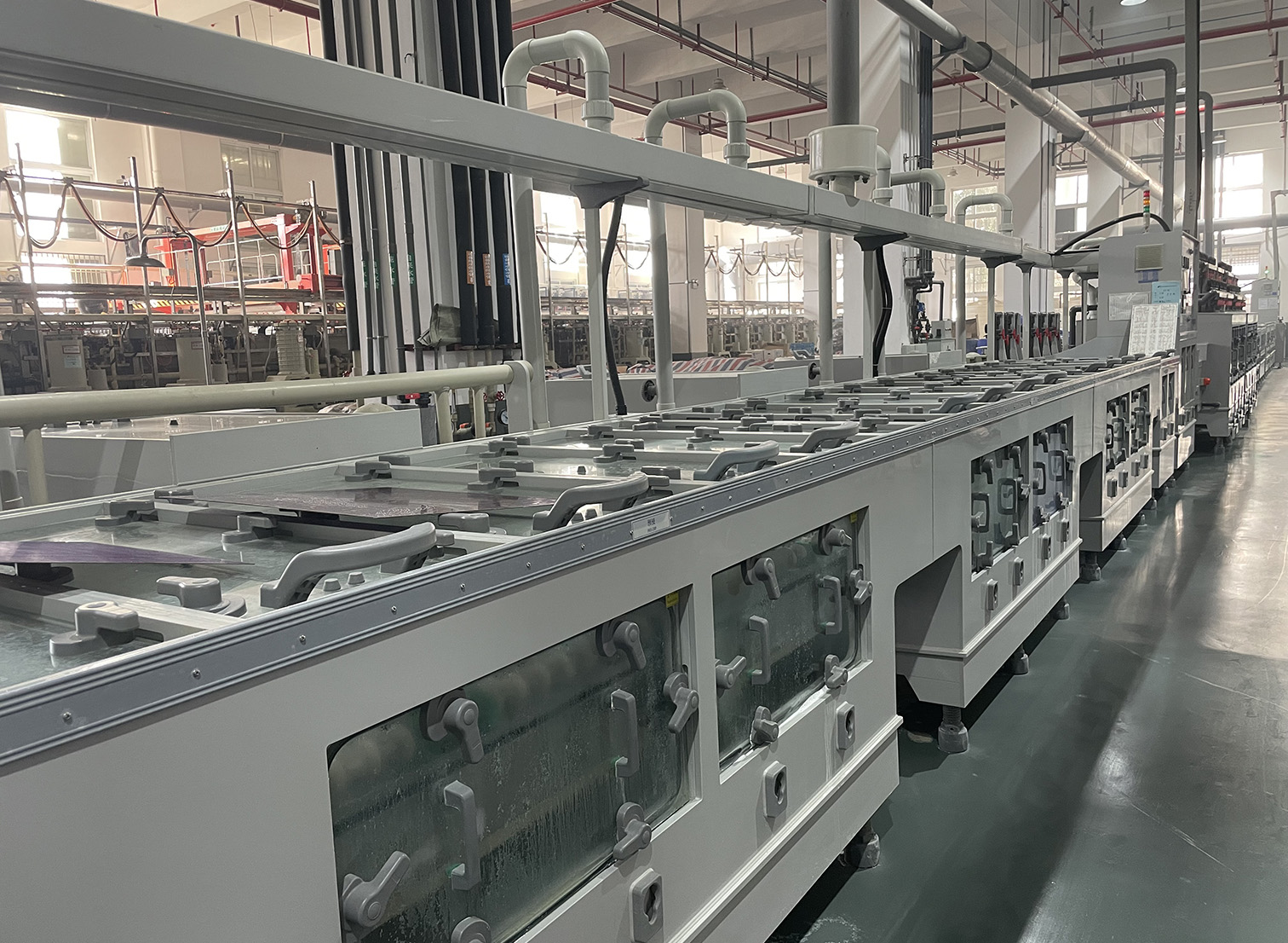
Over 20 years of PCB R&D, design and production, with a team of over 800 design engineers, striving for excellence — our service network has spread all over the world, delivering precision PCB solutions for EV charging infrastructure and powertrain systems globally.

As a company involved in the development and design of multiple scientific research products, our products are widely applied in various fields such as aviation, aerospace, automotive electronics, medical devices, industrial control, mobile terminal devices, servers, smart homes, AI applications, new energy, mini LED and testing instruments, etc.
We have a high-quality and highly capable technology R&D team, adhering to the development concept of high-end brands and products, and serving global customers. Our products are exported to various regions of the world. We continue to lead in the production of small batches, multiple varieties, high difficulty and high-precision products in differentiated market competition.
We have complete sets of advanced automatic production and testing equipment, strictly control every process, and are committed to the meticulous and perfect quality of products. All products strictly adopt international IPC standards for production and inspection, with 24-hour high quality one-on-one service.

We uphold the spirit of craftsmanship to build intelligent manufacturing, leading the industry with technology and driven by technological innovation. We'll strive for excellence and become a leader in the industry, continuously strengthening our core competitiveness and establishing a leading position in various fields.
In the rapidly evolving EV charging PCB market, our commitment to continuous R&D investment, advanced process development, and customer-centric engineering support positions us as the preferred PCB partner for global EV charging station manufacturers and EV powertrain system integrators.
Superior quality and excellent service meet clients' needs and ideas, help them win the market to achieve success — powering the future of EV mobility, one precision PCB at a time.
Every charging station PCB we deliver reflects our uncompromising commitment to honesty, transparency, and technical excellence — from first prototype to mass production.
We invest continuously in advanced PCB process development — from SiC-optimized power stage layouts to AI-integrated controller board designs — keeping our customers at the forefront of EV technology.
Superior quality and excellent service meet clients' needs and ideas, help them win the market to achieve success — with 24-hour one-on-one engineering support across all time zones.
Explore our full range of advanced PCB products engineered for EV charging stations, powertrain systems, and next-generation electronics.