Leave Your Message
0%

In the ever-changing world of electronics, making sure your High-Density Interconnect (HDI) PCB designs are both top-notch and reliable is more important than ever for manufacturers. Shenzhen Rich Full Joy Electronics Co., Ltd., a leading high-tech firm in China, really leads the way in this area. They're all about pushing boundaries and improving their skills, but they also play a big role in helping the industry grow as a key startup hub. In this guide, we’re going to dive into some essential strategies and best practices you can use to optimize HDI PCB design — stuff that'll help boost performance and make sure things stay reliable. As we go through these tips, I’ll point out how using advanced designs and materials can really make a difference in a tough, competitive market—leading to longer-lasting products and happier users.
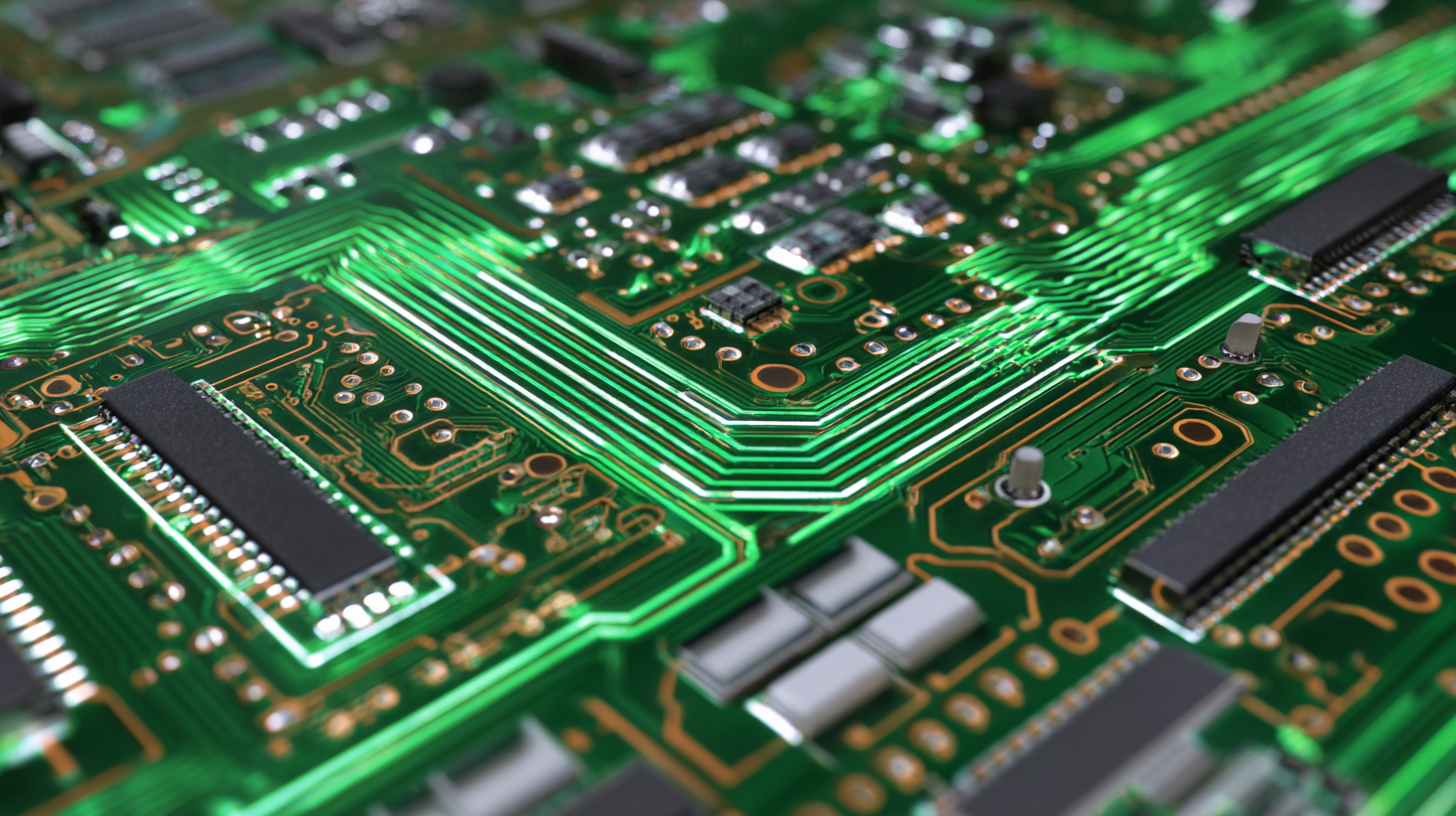
How to Optimize HDI PCB Design for Enhanced Performance and Reliability

Understanding HDI PCB Design: Key Principles for Reliability and Performance

You know, when it comes to designing High-Density Interconnect (HDI) PCBs these days, especially for things like cars and AI tech, it’s kinda like trying to pack as much as possible into as little space without losing performance. The key idea behind HDI PCB design is all about cramming in more circuits while keeping things reliable and running smoothly. Using fancy materials and techniques—stuff like blind and buried vias—really helps keep signals clear, which is super important since the automotive PCB market is booming. In fact, it’s expected to jump from around $9.15 billion in 2023 up to a hefty $15.1 billion by 2032.

When it comes to making these HDI PCBs work well, you’ve gotta pay attention to what materials you pick, how you stack the layers, and how you deal with heat. The materials you choose can really impact how well the board handles heat and how long it lasts—especially under tough conditions. As more industries jump into AI and the Internet of Things, nailing these design practices isn’t just a good idea, it’s essential. It means longer-lasting products and smoother operations. So, for engineers trying to keep up with all these fast-moving tech changes, mastering HDI PCB design is pretty much a must.

Critical Material Selection for Optimizing HDI PCB Performance

When it comes to optimizing High-Density Interconnect (HDI) PCB designs, picking the right materials is actually kinda key to making sure everything works smoothly and stays reliable. I read in a report by the IPC (that’s the Institute of Printed Circuits) that your choice of substrate directly affects both how well the electrical signals perform and how the thing handles heat. For example, using low-loss materials like Rogers or Teflon can really cut down on dielectric loss, which is a fancy way of saying it keeps the signals clearer—especially at those tricky high frequencies. Switching over to these advanced materials can boost performance by around 20%, which is super important these days with all the fast data speeds we’re after.

How to Optimize HDI PCB Design for Enhanced Performance and Reliability

Oh, and don’t forget about the conductive materials. They’re not just about good conductivity, but also how well the whole board deals with heat. Recent studies show that using high-purity copper can cut down resistance and help the board get rid of heat more efficiently, so it lasts longer. The IEEE even found that PCBs made with really pure copper can handle temperatures over 150°C without breaking a sweat—that’s perfect for applications that demand a lot. As manufacturers keep pushing to make things smaller and faster, paying attention to material choices isn't just important — it’s pretty much essential to building awesome HDI PCBs.

Best Practices in Layer Stack-Up Design for Enhanced Signal Integrity

When you're working on optimizing HDI PCB designs, one of the most important things to think about is how you stack your layers. Getting the layer stack-up right can really boost signal integrity and also cut down on crosstalk and electromagnetic interference—that’s a big deal! It’s generally a good idea to keep signal layers balanced, meaning you want them placed symmetrically around the ground and power planes. This setup helps in keeping the impedance controlled, which is super important for high-speed signals that need to stay clean and stable.

On top of that, using microvias can make a huge difference in routing and can even help shrink your overall PCB size. Microvias allow for more compact component placement and shorter signal paths, which is especially handy when you’re designing something small but still need good signal integrity. And don’t forget about blind and buried vias—they can really help optimize the stack-up by reducing the number of layers you need, while still making solid connections between different parts of the board. These tips and tricks aren’t just about performance; they also make your PCB more reliable, especially for the tougher applications out there. Bringing together the right mix of these strategies can help you create a solid, dependable PCB that meets modern electronics' high standards.

How to Optimize HDI PCB Design for Enhanced Performance and Reliability

Layer Type Function Material Thickness (mm) Signal Layer Count
Signal Layer High-Speed Signal Transmission FR-4 0.1 4
Power Layer Power Distribution Copper 0.35 1
Ground Layer Ground Reference Copper 0.25 1
Via Layer Interlayer Connections FR-4 0.08 1

Thermal Management Strategies in HDI PCB to Prevent Failure

When it comes to designing high-density interconnect (HDI) printed circuit boards (PCBs), managing heat isn’t just a minor detail — it’s totally crucial. With electronics getting smaller and more powerful than ever, all these densely packed components tend to generate a ton of heat, which can really affect how well everything works and how reliable the device is. That’s why having good thermal management strategies in place is a must if we want our gadgets to perform at their best without heating up too much.

One way to tackle this is by using advanced materials that are better at conducting heat and helping it spread out. Things like clever heat sinks and thermal vias can really make a difference in kicking heat away from critical areas. Plus, paying attention to how you lay out the components can help improve airflow — which is basically nature’s way of cooling things down.

And here’s a neat trick: during the design process, using simulation tools can help predict potential heat-related issues before you even get to production. This way, engineers can tweak things early on, making sure the final product isn’t just cool in terms of design but also reliable and capable of handling the heat.

On top of that, more and more designers are turning to AI to make thermal management even smarter. AI can analyze complex heat patterns and suggest adjustments that might not be obvious at first glance. By tapping into these cutting-edge technologies, PCB designers can come up with solutions that not only meet the lofty demands of modern electronics but also stand up to the heat — literally — in that challenging environment. It’s all about staying one step ahead when it comes to performance and reliability.

Utilizing Simulation Tools for Accurate HDI PCB Performance Prediction

When it comes to designing high-density interconnection (HDI) PCBs, using simulation tools really makes a difference. These days, many designers rely on advanced simulation software to predict how their boards will perform and how reliable they'll be — before even building a single prototype. It’s a huge time saver and helps cut down costs, too.

My tip? Start with a detailed model of your PCB layout. Make sure all the components and connections are spot-on, because that’s where most issues happen. Also, use simulation tools that can check signal integrity, heat flow, and electromagnetic interference — doing this gives you a full picture of how your design will behave in real life. Taking this proactive approach means catching problems early, rather than fixing them later.

And don’t forget to test and tweak as you go. Instead of waiting until everything’s finished, run simulations with different configurations or materials to see what works best. This ongoing feedback loop helps you fine-tune your design, leading to a final product that’s not only high-performing but also super reliable — perfect for today’s fast-paced tech world.

How to Optimize HDI PCB Design for Enhanced Performance and Reliability

Emerging Trends and Technologies in HDI PCB Manufacturing and Design

In the fast-changing world of HDI PCB manufacturing, keeping up with the latest trends and tech is pretty much essential if you want your designs to perform well and stay reliable. One really big development lately is the use of more advanced materials, like high-frequency laminates and thermally conductive substrates. These not only boost the electrical performance of your PCBs but also help a lot with heat dissipation — which is super important, especially for high-speed stuff.

Tip: It’s a good idea to start thinking about using these advanced materials early on in your design process. That way, you can make sure they play nicely with your circuit requirements and thermal management plans.

Another cool trend is the rise of automated design tools powered by AI. These can make your life way easier by catching potential issues early, helping you optimize your layouts, and even running simulations to see how things will perform. All of this saves time and can help you avoid costly mistakes down the line. Incorporating these kinds of tools can really up your game in design efficiency and reliability.

Tip: Do some research to find automation tools that suit your specific project needs, and make sure to take the time to train your team on how to get the most out of them. Trust me, it’s worth it.

FAQS

: What is the impact of material selection on HDI PCB performance?

: The choice of substrate material, such as low-loss materials like Rogers or Teflon, significantly influences electrical performance and thermal management, potentially improving performance metrics by up to 20% for high-speed applications.

How does conductive material influence HDI PCB reliability?

Using high-purity copper minimizes resistance and improves heat dissipation, allowing PCBs to operate efficiently at temperatures exceeding 150°C, thus prolonging their lifespan.

What role does layer stack-up design play in HDI PCBs?

A well-structured layer stack enhances signal integrity, minimizes crosstalk, and reduces electromagnetic interference, crucial for high-speed signal transmission.

What are some best practices for layer stack-up configuration?

Designers should create a balanced stack-up with signal layers placed symmetrically around ground and power planes, and incorporate microvias, blind, and buried vias to optimize routing and reduce layer count.

Why are microvias important in HDI PCB design?

Microvias improve routing efficiency and allow for tighter placement of components, maintaining signal integrity in compact designs due to shorter signal paths.

How can simulation tools benefit HDI PCB designers?

Simulation tools enable designers to predict performance and reliability by assessing electrical and thermal characteristics before physical prototyping, reducing development time and costs.

What should be considered when using simulation tools for HDI PCBs?

Start with a comprehensive model, accurately represent all components, and use tools that simulate signal integrity, thermal management, and electromagnetic interference for a holistic performance view.

What is the importance of iterative testing in the HDI PCB design process?

Conducting iterative testing allows designers to simulate different configurations or materials throughout the design phase, facilitating optimization of performance and reliability before final production.

How does the choice of materials affect thermal management in HDI PCBs?

The use of advanced materials with better thermal properties can greatly enhance heat dissipation, preventing potential overheating and enhancing the overall reliability of the PCB.

What is the correlation between signal integrity and layer design in HDI PCBs?

The design of the layer stack directly affects signal integrity, and a balanced stack-up helps maintain controlled impedance necessary for effective high-speed signal transmission.

Conclusion

In today’s fast-paced electronics world, tweaking HDI PCB designs is pretty much essential if you wanna boost performance and keep things reliable. Getting a good grip on the main principles behind HDI PCB design helps engineers craft high-density interconnect boards that actually meet the crazy demanding needs of modern tech. Picking the right materials is a big deal too — it can make or break how well your board performs. And don’t forget, following best practices when it comes to layer stack-up design really helps maintain signal quality and integrity.

On top of that, managing heat effectively is super important to avoid failures down the line and to make your PCBs last as long as possible. Using advanced simulation tools can give you a pretty accurate idea of how your design will perform, so you can spot and fix potential issues before hitting production. As Shenzhen Rich Full Joy Electronics Co., Ltd. points out, keeping up with the latest trends and tech in HDI PCB manufacturing can really push your product’s design and reliability to the next level.
Liam

Liam

Liam is a dedicated marketing professional at Shenzhen Ruizhixinfeng Electronics Co., Ltd., where he leverages his extensive expertise in the electronics industry to drive the company's communication strategy. With a deep understanding of the latest technological advancements and market trends,......
Previous Future Trends in High Frequency Pcb Technology for Global Buyers