
0102030405


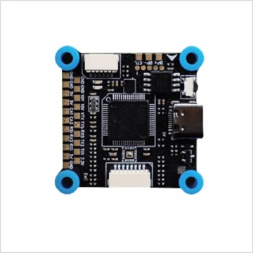
3D Ultra-Wideband Frequency Synthesizer PCB: Precision Engineered for High-Performance Applications


Features of PCB Products:

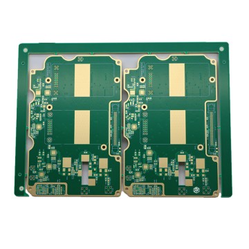
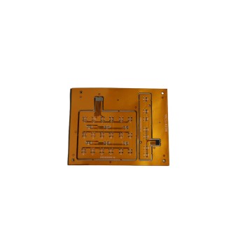
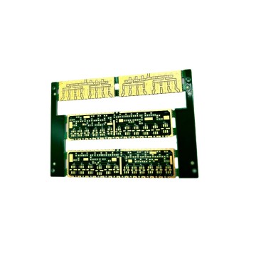
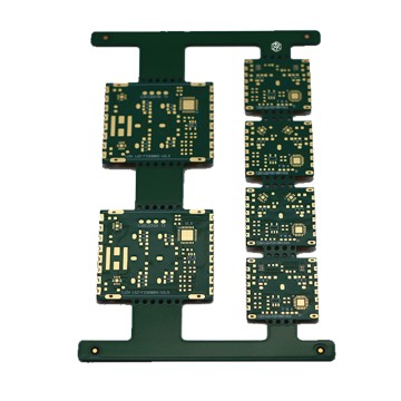
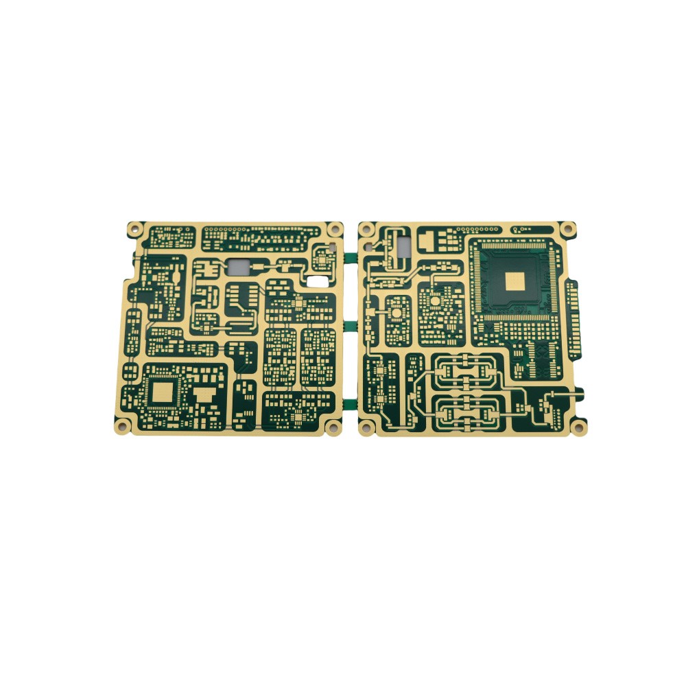
●Type: Multi-layer PCB with high-frequency mixed-pressure technology
●Material: High-frequency materials, TG170 FR-4, RO4350B, S1000-2M
●Number of Layers: 6L
●Board Thickness: 1.1mm
●Surface Finish: Nickel-Palladium-Gold
●Special Features: Blind vias, back drilling, resin-filled vias
●Drilling: 3 times
●Lamination: 1 time
Design and Product Features:
●Advanced High-Frequency Mixed-Pressure Technology: Ensures optimal signal integrity and performance.
●Blind Vias and Back Drilling: Enhance signal transmission and reduce interference.
●Resin-Filled Vias: Improve mechanical strength and reliability.
●Nickel-Palladium-Gold Finish: Provides excellent conductivity and corrosion resistance.
Why Choose This PCB?
●High Precision: Manufactured with one precise lamination and three meticulous drilling steps, ensuring every layer is perfectly aligned and every via is accurately placed. This meticulous process guarantees the highest level of precision, making it ideal for demanding high-frequency applications where accuracy is paramount.
●Unique Special Processes: Our PCB stands out with exceptional performance and reliability. The incorporation of advanced high-frequency mixed-pressure technology, combined with blind vias, back drilling, and resin-filled vias, enhances signal integrity and reduces interference. These unique processes not only improve the mechanical strength and reliability of the board but also ensure long-term durability in high-performance environments.
●Balanced Design: The combination of high-frequency materials like TG170 FR-4, RO4350B, and S1000-2M, along with precise thickness control, achieves a total thickness of 1.1mm. This balanced design ensures optimal performance without compromising on the compactness required for modern electronic devices. The six-layer structure, with a fine nickel-palladium-gold finish, further enhances conductivity and corrosion resistance, making it suitable for a wide range of precision applications.

●Superior Performance and Reliability: By integrating these advanced features and processes, our 3D Ultra-Wideband Frequency Synthesizer PCB delivers superior performance and reliability. Whether you are developing cutting-edge communication systems, high-precision radar equipment, or advanced medical imaging devices, this PCB is engineered to meet the most stringent requirements. Choose us for your high-frequency needs and experience the difference in quality and performance.
In - depth Analysis: Key Questions and Answers about Nickel - Palladium - Gold Treatment of Printed Circuit Boards

Why is the nickel-palladium-gold treatment so important for the electrical conductivity of printed circuit boards (PCBs)?
Answer: In the nickel-palladium-gold treatment, the gold layer has extremely high electrical conductivity, which can greatly reduce the resistance of electron transmission and ensure the rapid and accurate transmission of signals. The nickel layer also has a certain degree of electrical conductivity, laying the foundation for signal transmission. Moreover, good electrical conductivity is crucial for 3D ultra-wideband very small step frequency hopping frequency synthesis PCBs, which can ensure the efficient transmission of high-frequency signals and reduce signal attenuation and distortion.
How does the nickel-palladium-gold treatment improve the corrosion resistance of PCBs?
Answer: The nickel layer adheres to the base material, providing preliminary protection. The palladium layer has high chemical stability. As a transition layer, it enhances the bonding force and resists the erosion of chemical substances. The gold layer covers the outermost layer, and its excellent corrosion resistance can effectively prevent the PCB from being oxidized and corroded in humid, acidic, alkaline and other environments, thus extending the service life of the PCB.
How to precisely control the thickness of each layer of nickel, palladium and gold?
Answer: To precisely control the thickness of each layer of nickel, palladium and gold, it is necessary to start from multiple aspects. First of all, the composition of the plating solution should be accurately prepared. According to the requirements of different plating layers, the proportions of nickel salts, palladium salts, gold salts and additives in the plating solution should be strictly controlled. Secondly, the electroplating parameters such as current density, electroplating time, temperature, etc. should be precisely set and monitored in real time, and the optimal parameters should be determined through repeated experiments and experience accumulation. At the same time, advanced automatic electroplating equipment with high-precision parameter control and stable operation performance should be adopted to ensure the consistency of the thickness of each layer.
What is the impact of the change in the thickness ratio of each layer of nickel, palladium and gold on the performance of PCBs?
Answer: If the nickel layer is too thick, although it can enhance the bonding force with the base material, it may affect the overall electrical conductivity; if it is too thin, the bonding force is insufficient, and the plating layer is likely to fall off. The change in the thickness of the palladium layer affects its effect as a transition layer. If it is too thick, it may increase the cost and affect the signal transmission performance; if it is too thin, it cannot effectively enhance the bonding force and corrosion resistance. If the gold layer is too thick, it will increase the cost. If it is too thin, the electrical conductivity and corrosion resistance cannot be fully utilized, which may lead to signal attenuation and the PCB being vulnerable to corrosion, affecting the service life and performance stability.
How is the corrosion resistance of PCBs treated with nickel-palladium-gold in different environments?
Answer: In a general indoor dry environment, the PCB treated with nickel-palladium-gold can maintain a good state for a long time, and the corrosion resistance effect is remarkable, which can effectively prevent natural oxidation. In a humid environment, due to the protection of the gold layer and the palladium layer, it can resist a certain degree of water vapor erosion. However, if it is in a high-humidity environment for a long time, there may be slight signs of corrosion. In a chemical corrosion environment such as strong acids and alkalis, although it has a certain corrosion resistance, with the passage of time and the increase in the concentration of the corrosive medium, the PCB may be gradually corroded, affecting its performance and service life.
How to ensure the consistency of the quality of nickel-palladium-gold treatment in mass production?
Answer: In mass production, it is necessary to ensure the stability of the composition of the plating solution, regularly detect and supplement the components of the plating solution, and maintain the consistency of its concentration and performance. Regularly maintain and calibrate the electroplating equipment to ensure the accuracy and stability of the equipment parameters. Strictly train the operators to make them proficient in the electroplating process and operation specifications, and reduce the differences caused by human factors. At the same time, establish a perfect quality inspection system, randomly inspect each batch of PCBs, and promptly discover and correct quality problems.
What is the impact of the nickel-palladium-gold treatment on the solderability of PCBs?
Answer: The nickel-palladium-gold treatment can significantly improve the solderability of PCBs. The nickel layer provides a good soldering foundation, and the palladium layer can prevent the oxidation of nickel and ensure the activity of the surface of the nickel layer during soldering. The gold layer has good wettability, which can help the solder spread and adhere better, making the soldering process smoother and the solder joints more secure, thus improving the reliability of the connection between the PCB and electronic components.
How to clean and maintain the PCB after the nickel-palladium-gold treatment?
Answer: The treated PCB should avoid contact with sharp objects to prevent scratching the plating layer. When cleaning, special electronic cleaning agents can be used, and gentle methods such as gently brushing with a soft brush or spray cleaning with a spray gun can be adopted to remove impurities such as dust and oil stains on the surface. Avoid using highly corrosive cleaning agents to prevent damage to the nickel-palladium-gold plating layer. In terms of maintenance, store the PCB in a dry and well-ventilated environment, control the humidity within an appropriate range, avoid long-term exposure to a high-humidity or chemically polluted environment, and regularly check whether there are any abnormalities on the surface of the PCB, such as discoloration, signs of corrosion, etc.
Applications of 3D Ultra-Wideband Frequency Synthesizer PCB

The 3D Ultra-Wideband Frequency Synthesizer PCB, with its advanced high-frequency mixed-pressure technology, blind vias, back drilling, and resin-filled vias, is designed to meet the stringent requirements of various high-performance applications. Here are ten detailed applications where this PCB excels:
1.5G Infrastructure:
●Base Stations: The high-frequency materials and precise manufacturing processes ensure optimal signal integrity and minimal interference, making it ideal for 5G base stations that require high-speed data transmission and low latency.
●Small Cells: Used in small cell deployments to enhance network coverage and capacity in urban and dense environments.
2.Automotive Radar Systems:
●ADAS (Advanced Driver-Assistance Systems): The PCB’s ability to handle high-frequency signals with minimal loss makes it suitable for radar systems in autonomous vehicles, providing precise distance and speed measurements.
●Collision Avoidance Systems: Ensures reliable performance in critical safety applications, reducing the risk of accidents.
3.Medical Imaging Devices:
●MRI Machines: The PCB’s high-frequency capabilities and precise signal transmission are crucial for generating detailed internal body images, aiding in accurate medical diagnoses.
●Ultrasound Equipment: Provides high-resolution imaging by ensuring stable and clear signal transmission, enhancing diagnostic accuracy.
4.Aerospace and Defense:
●Satellite Communication: Used in satellite communication systems for reliable and high-speed data transmission, ensuring stable communication links.
●Avionics: Critical for flight control systems and navigation equipment, where high reliability and performance are paramount.
5.High-Speed Digital Boards:
●Network Switches: Enhances signal integrity and reduces EMI in high-speed digital boards, making it suitable for network switches and other telecom systems.
●Optical Transceivers: Ensures high-speed data transmission with minimal signal loss, ideal for optical transceiver modules.
6.RF and Microwave Circuits:
●Telecommunication: Reduces EMI and improves signal clarity in RF and microwave circuits, essential for telecommunication and aerospace applications
●Broadband Amplifiers: Provides stable performance across a wide frequency range, making it suitable for broadband amplifiers used in various RF applications
7.Industrial Automation:
●High-Frequency Sensors: Ensures reliable and accurate signal transmission in industrial sensors, enhancing the efficiency and precision of automation systems.
●Control Systems: Used in high-speed control systems for real-time monitoring and control of industrial processes.
8.Consumer Electronics:
●Smartphones and Tablets: The compact design and high-frequency performance make it suitable for advanced consumer electronics, ensuring high-speed data processing and communication.
●Smart Home Devices: Used in Wi-Fi routers, smart thermostats, and security systems, providing reliable wireless connectivity and data transmission.
9.Research and Development:
●Laboratory Equipment: Ensures precise signal transmission and high reliability in research and development applications, such as high-frequency test and measurement equipment.
●Experimental Systems: Provides stable performance in experimental setups requiring high-frequency signal processing and data acquisition.
10.Military and Defense:
●Electronic Warfare Systems: Ensures high reliability and performance in critical military applications, such as electronic warfare and secure communication systems.
●Guidance Systems: Used in missile guidance systems and other military applications where high precision and reliability are essential.
Quality Assurance:
●Strict Quality Inspection: Comprehensive testing to ensure performance and reliability.
●Traceability System: Detailed records from raw material to finished product.
More Knowledge about High-Frequency PCBs:
●Importance of High-TG Material: Ensures stability and performance in high-temperature environments.
●Benefits of Nickel-Palladium-Gold Finish: Enhances conductivity and durability.
●Advantages of Blind Vias and Back Drilling: Improves signal integrity and reduces interference.
The 3D Ultra-Wideband Frequency Synthesizer PCB, with its advanced features and high-performance capabilities, is designed to meet the demanding requirements of modern high-frequency applications. Whether in 5G infrastructure, automotive radar systems, medical imaging devices, or aerospace and defense, this PCB delivers superior performance and reliability. Choose us for your high-frequency needs and experience the difference in quality and performance.