0102030405
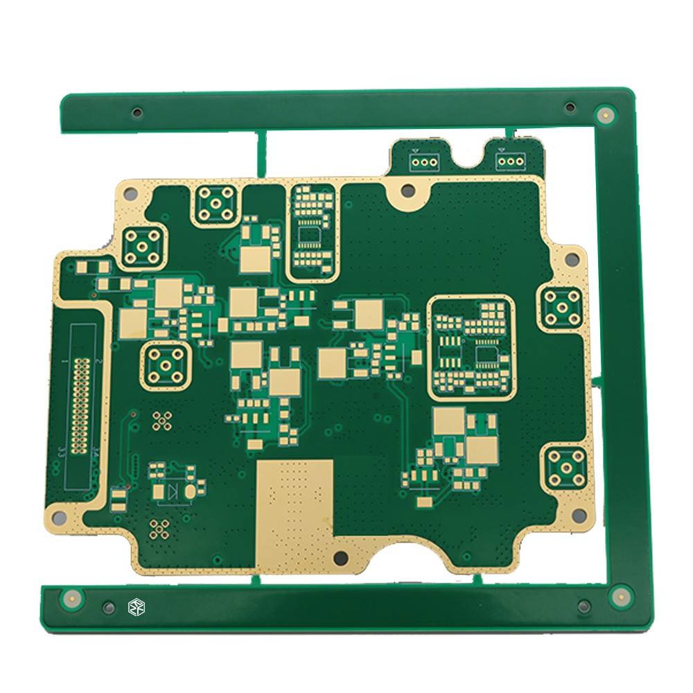
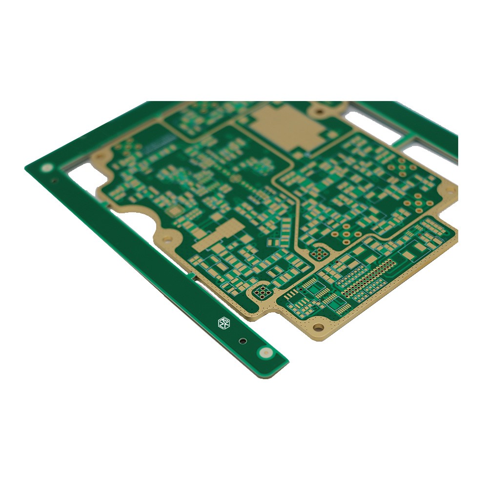
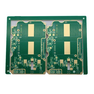
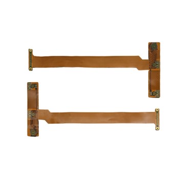
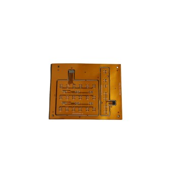
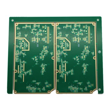
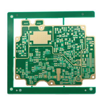
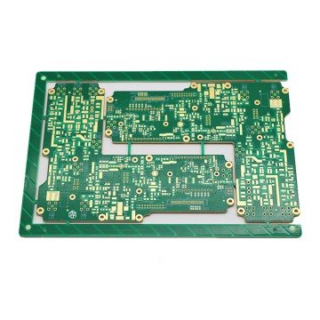
6-Layer High-Frequency PCB | Rogers RO4350B | Metal Edge Shielding & Resin Plugged Vias


Design and Product Features
Product Specifications
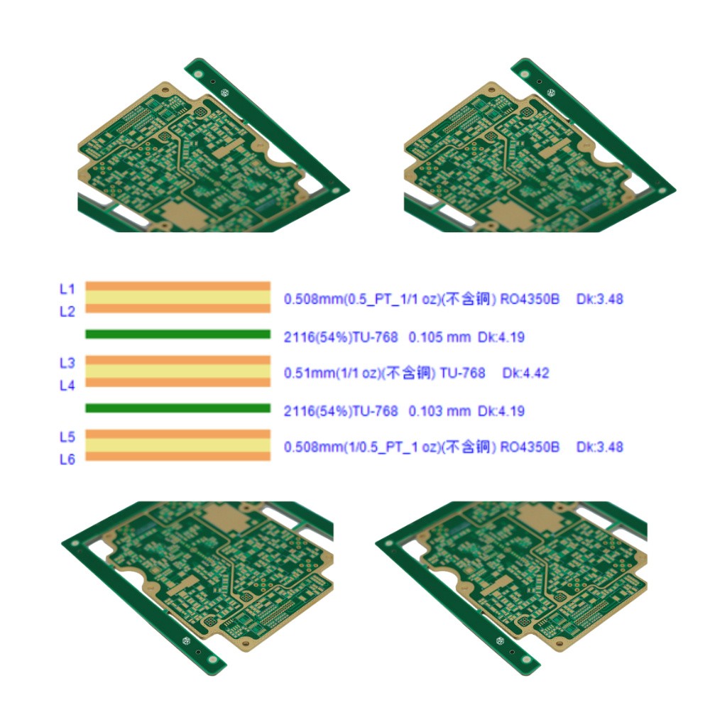
PCB | impedance | resin plug hole Materia Rogers RO4350B+Regular Substrates S1000-2M、FR-4、TG170
Number of layer 6L
Board Thickness 2.0mm
Single size 123*132mm/1PCS
Surface finish ENIG
Inner copper thickness 35um
Outer copper thickness 35um
Color of solder mask green(GTS,GBS)
Silkscreen color white(GTO,GBO)
Via treatment resin plug hole
Density of mechanical drilling hole 14W/㎡
Min via size 0.2mm
Min line width/space 8/5mil
Aperture ratio 10mil
Pressing times 1 time
Drilling times 1 time
Advantages of Innovative Material Combination
Our PCB innovatively combines materials such as Rogers RO4350B, S1000 - 2M, FR - 4, and TG170. Rogers RO4350B, with its excellent low - loss characteristics, ensures efficient high - frequency signal transmission. S1000 - 2M enhances the overall electrical performance, FR - 4 provides stable mechanical support, and TG170 ensures the PCB can operate stably in high - temperature environments. This unique material combination enables the PCB to maintain excellent electrical and mechanical properties under complex working conditions, meeting the growing demands of high - end electronic products.
Metal Edging and Electromagnetic Shielding Design
The metal edging design is a major highlight of this PCB. The metal edging not only enhances the mechanical strength of the PCB but also serves as a natural electromagnetic shielding layer. During high - frequency signal transmission, it can effectively block external electromagnetic interference from entering the PCB and prevent internal signals from leaking out, greatly improving the stability and confidentiality of signal transmission. It is especially suitable for application scenarios with extremely high requirements for electromagnetic compatibility, such as military communication equipment and high - end medical diagnostic instruments.
Advanced Resin Plug Hole Process
The advanced resin plug hole process we adopt brings many benefits to the performance improvement of the PCB. The resin plug holes fill the vias, effectively avoiding problems such as solder balls and short - circuits during the soldering process and improving the production yield. At the same time, the filled resin enhances the mechanical strength of the vias, ensuring the reliability of the electrical connections between multiple layers of the PCB. In addition, the good insulation performance of the resin further reduces signal loss and interference at the vias, improving the overall performance of the PCB in high - frequency circuits.
High - Precision Manufacturing Process
This PCB demonstrates high - precision manufacturing processes. The high mechanical drilling density of 14W/㎡, the minimum via size of 0.2mm, and the minimum line width/space of 8/5mil reflect our excellent skills in the PCB manufacturing field. High - precision manufacturing ensures a more compact and reasonable component layout on the circuit board, improving the integration level. At the same time, precise circuit layout and copper thickness control effectively reduce signal transmission delay and loss, providing a solid guarantee for the stable transmission of high - speed and high - frequency signals.
Millimeter Circuit Board Performance Highlights
Exceptional High - Frequency Performance
With advanced materials and a carefully designed circuit structure, this PCB performs exceptionally well in high - frequency applications. Precise impedance control, combined with low - loss materials, minimizes signal attenuation during transmission and can stably support high - frequency band signal transmission. Whether it's the millimeter - wave band in 5G communication or the ultra - high - frequency signals in satellite communication, it can be processed efficiently, meeting the strict requirements of modern communication technologies for high - frequency PCBs and providing a reliable guarantee for high - speed data transmission.
High Reliability and Stability
Every link, from material selection to the manufacturing process, is strictly controlled to ensure the high reliability and stability of the PCB. Multiple strict quality inspections, including electrical performance tests and environmental adaptability tests, simulate various extreme usage environments to verify the performance of the PCB. Even under harsh conditions such as high temperature, low temperature, humidity, and strong electromagnetic interference, the PCB can still maintain stable electrical and mechanical properties, providing solid support for the long - term stable operation of electronic products.
High Integration and Multifunctionality
Through high - precision manufacturing processes and optimized circuit design, this PCB achieves high integration and multifunctionality. The small line width/space and via size allow the circuit board to accommodate more electronic components, realizing more functions in a limited space. Whether it's complex digital circuits, analog circuits, or radio - frequency circuits, they can be perfectly integrated on this PCB, meeting the trend of electronic products towards miniaturization and multifunctionality.
Why is metal edging designed for PCBs?
In PCB design, the use of metal edging (high - frequency hybrid metal edge) is mainly due to the following reasons:
1. Meet special application requirements
●Compliance with industry standards and regulations: In certain industries such as military and medical, there are extremely high requirements for the safety, reliability, and electromagnetic compatibility of electronic devices. PCBs designed with metal edging are more likely to meet these industry standards and specifications. For example, military equipment performs tasks in complex electromagnetic environments, and metal edged PCBs can provide better electromagnetic shielding and structural protection, ensuring that the equipment works properly in extreme environments.
●Adapt to harsh environments: Metal edging can provide additional protection for PCBs in harsh conditions such as high temperature, humidity, and corrosive environments. Metal edging can prevent corrosion of PCB edges and extend the lifespan of the PCB. In the electronic equipment of offshore oil extraction platforms, metal edging can effectively resist the erosion of sea winds and ensure the stable operation of PCBs.
2. Enhance mechanical performance
●Improve structural strength: Metals have high strength and hardness, providing additional mechanical support for the PCB. In high - frequency hybrid PCB applications, the device may be subjected to external forces such as vibration and impact. The metal edging can effectively reduce the risk of deformation and fracture of the PCB caused by external forces. For example, in the aerospace field, aircraft experience strong vibrations during flight. PCBs with metal edging can better adapt to this environment and ensure the stable operation of electronic devices.
●Facilitate installation and fixation: The metal edging can increase the reliability of the connection between the PCB and other equipment or the housing. By connecting the metal edging to the equipment frame through screws, welding, etc., the PCB can be installed more firmly in the device, preventing the loosening from affecting the electrical connection performance and ensuring that the high - frequency signal transmission is not interfered with.
3. Optimize electrical performance
●Electromagnetic shielding: High - frequency hybrid PCBs are often used to process high - frequency signals. High - frequency signals are prone to being interfered with by external electromagnetic fields during transmission and may also radiate out to interfere with other electronic components. The metal edging can serve as an electromagnetic shielding layer. Utilizing the electrical and magnetic conductivity of the metal, it can shield external electromagnetic interference from the PCB and prevent the internal signals of the PCB from leaking. For example, in 5G communication base stations, the metal edging can effectively reduce electromagnetic interference between different modules and ensure stable communication signal transmission.
●Improve grounding effect: The metal edging is connected to the grounding layer of the PCB, which can expand the grounding area, reduce the grounding resistance, and improve the grounding effect. This is crucial for optimizing the return path of high - frequency signals, reducing signal reflection and loss, and enhancing signal integrity. In automotive radar systems, a good grounding design combined with metal edging can ensure the accurate transmission and reception of millimeter - wave signals and improve the detection accuracy of the radar.
4. Enhance heat dissipation capacity
●Conduct heat quickly: Metals have good thermal conductivity. When the high - frequency hybrid PCB is working, the metal edging can quickly conduct the heat generated on the PCB. With the continuous improvement of the integration of electronic devices, the heat - generation problem has become more prominent. Especially, high - frequency circuits generate a large amount of heat during operation. The metal edging can effectively share the heat - dissipation task of the PCB, conduct the heat to the device housing or the heat - dissipation device, and prevent the performance degradation or damage of the PCB due to overheating, ensuring the long - term stable operation of the electronic device.
5. Meet special application requirements
●Comply with industry standards and specifications: In some specific industries, such as the military and medical fields, the requirements for the safety, reliability, and electromagnetic compatibility of electronic devices are extremely high. PCBs with metal edging design can more easily meet these industry standards and specifications. For example, military equipment performs tasks in a complex electromagnetic environment. PCBs with metal edging can provide better electromagnetic shielding and structural protection, ensuring the normal operation of the equipment in extreme environments.
●Adapt to harsh environments: In harsh conditions such as high - temperature, humid, and corrosive environments, the metal edging can provide additional protection for the PCB. The metal edging can prevent the edge of the PCB from being corroded and extend the service life of the PCB. In the electronic equipment on offshore oil - drilling platforms, the metal edging can effectively resist the erosion of sea breeze and ensure the stable operation of the PCB.
Advantages and disadvantages of metal edging in PCB design
In PCB design, metal edging is a widely - used design choice, which has many advantages as well as some disadvantages that cannot be ignored.
1.Advantages
●Enhanced Electromagnetic Shielding Effect: The metal edging can act like a barrier, effectively blocking external electromagnetic interference from entering the interior of the PCB and preventing the electromagnetic signals generated by the PCB itself from leaking out. In communication devices and medical electronic devices with strict requirements for electromagnetic compatibility, the metal edging can avoid signals being interfered by external clutter, ensuring the accuracy and stability of signal transmission. It also prevents the electromagnetic radiation of the device itself from affecting other devices.
●Increased Mechanical Strength: Metal materials have high strength, providing additional physical support for the PCB. In some application scenarios where vibration and impact may be encountered, such as automotive electronics and aerospace fields, the metal edging can reduce the risk of the PCB being deformed or damaged by external forces, ensuring the normal operation of the circuits and components on the PCB.
●Optimized Heat Dissipation Performance: The good thermal conductivity of metal enables the metal edging to quickly dissipate the heat generated during the operation of the PCB. With the increasing integration of electronic devices, the heat - generation problem has become more prominent. The metal edging can serve as an auxiliary heat - dissipation path, conducting heat to the device housing or heat - dissipation devices, improving the overall heat - dissipation efficiency of the system and preventing the PCB from suffering performance degradation or malfunction due to overheating.
●Improved Grounding Performance: The metal edging is usually connected to the grounding layer of the PCB, which expands the grounding area, reduces the grounding resistance, and optimizes the grounding effect. This is crucial for stabilizing the potential of the circuit and reducing signal reflection and interference. Especially in high - speed and high - frequency circuits, good grounding helps to improve signal quality and system stability.
2.Disadvantages
●Increased Cost: Using metal edging incurs additional material costs. Moreover, during the manufacturing process, its processing technology is relatively complex, which may involve special stamping, welding, or cladding processes, further increasing the production cost. For some products with strict cost control requirements, the application of metal edging may be restricted.
●Increased Weight: Metals have a relatively high density. Adding metal edging to the PCB will increase the overall weight. In application scenarios with strict weight requirements, such as drones and wearable devices, excessive weight may affect the portability and energy consumption of the device. Therefore, the use of metal edging needs to be carefully considered.
●Higher Design and Manufacturing Difficulty: The design of metal edging requires considering its compatibility with other parts of the PCB, such as the connection between the metal edging and the circuit layers, and the impact of the thickness and shape of the metal on signal transmission. During the manufacturing process, ensuring the dimensional accuracy and connection reliability of the metal edging requires high - level production equipment and technologies. If the design or manufacturing is improper, problems such as short - circuits and open - circuits may occur, reducing the product yield.
●Possible Signal Coupling Issues: In high - frequency circuits, the metal edging may cause signal coupling with the circuits on the PCB. This coupling may change the signal transmission characteristics, generating additional signal reflections or interferences and affecting signal integrity. Therefore, when using metal edging in high - frequency PCB design, accurate electromagnetic simulation and optimized design are required to reduce such adverse effects.
Why Choose Our High - Frequency Hybrid & Metal Edging PCB?
Professional R & D and Manufacturing Team
We have a professional R & D and manufacturing team. Team members have rich experience and profound professional knowledge in the PCB field. R & D personnel constantly explore new materials and processes, aiming to improve product performance. The manufacturing team uses advanced production equipment and strict process flows to ensure that each PCB meets high - quality standards. The support of the professional team is a strong guarantee for the quality and innovation of our products.
Customized Services and Flexible Production
We understand that each customer's needs are unique, so we provide customized services. No matter what special requirements customers have for the number of layers, size, and functional modules of the PCB, or if they need specific material combinations and surface treatment processes, we can carry out customized production according to customer needs. The flexible production model ensures that we can quickly respond to customer needs, provide personalized solutions, and help customers stand out in the market competition.
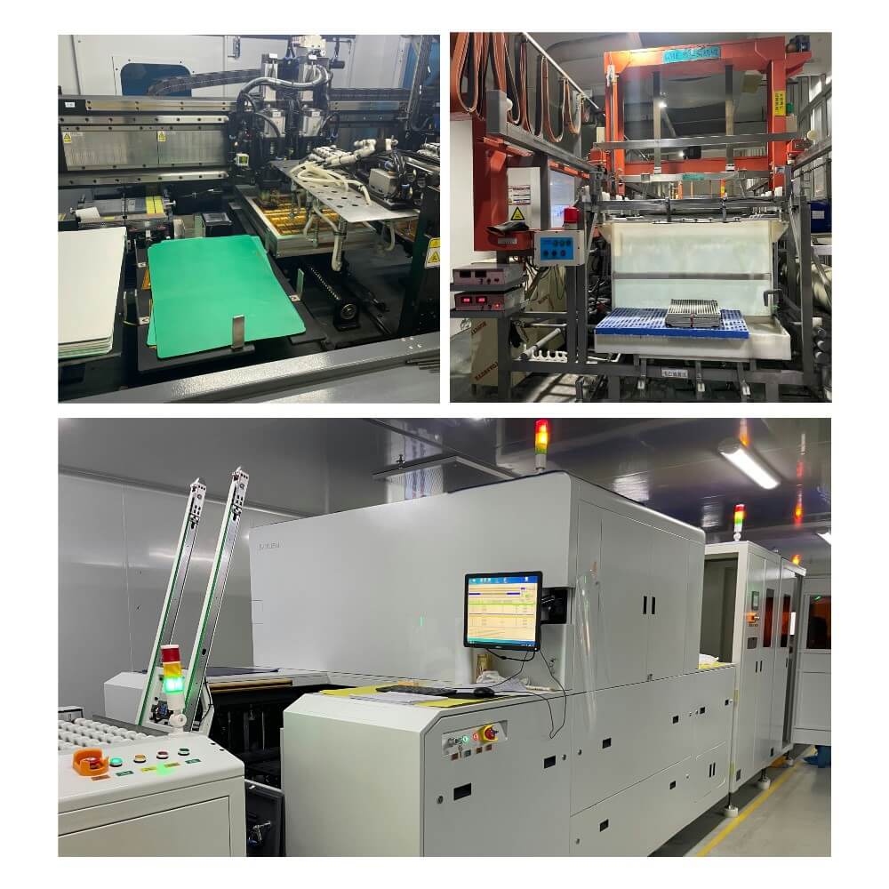
Strict Quality Control System
We have established a complete and strict quality control system. Every link, from raw material procurement to finished product delivery, is strictly inspected. Comprehensive performance tests are carried out on raw materials to ensure their quality meets the standards. During the production process, key process parameters are monitored in real - time to ensure product consistency. Before the finished product leaves the factory, multiple performance tests, such as 100% impedance testing and X - ray inspection, are carried out to ensure that each PCB meets high international standards, allowing customers to use them with confidence.
Millimeter Circuit Board Quality Assurance
Strict Raw Material Screening
We are extremely strict in screening raw materials and only select material suppliers that meet high standards. For key materials such as Rogers RO4350B and S1000 - 2M, strict electrical and physical performance tests are carried out. Each batch of raw materials undergoes multiple inspection processes to ensure its stable and reliable quality, eliminating product defects caused by raw material problems from the source and laying a solid foundation for producing high - quality PCBs.
Full - Process Monitoring of the Production Process
During the production process, we use an advanced production management system to monitor every link in the whole process. The key parameters of each process, from drilling, pressing to circuit etching, are accurately recorded and strictly controlled. Through real - time monitoring, problems that occur during the production process can be promptly discovered and solved, ensuring the stability and consistency of product quality, improving production efficiency, and ensuring the timely delivery of high - quality products.
Complete Finished Product Detection Mechanism
We have a complete finished product detection mechanism and conduct comprehensive inspections on each PCB. In addition to regular electrical performance tests and appearance inspections, reliability tests such as high - and low - temperature cycle tests, humidity tests, and vibration tests are also carried out. By simulating the actual usage environment, the performance of the PCB is comprehensively evaluated to ensure that the product can work properly under various conditions, providing reliable product guarantees for customers.
What are the application scenarios of PCBs with metal edging?
PCB with metal edging, leveraging its unique properties, plays a crucial role in multiple fields and has a wide range of application scenarios:
1.Communication Field
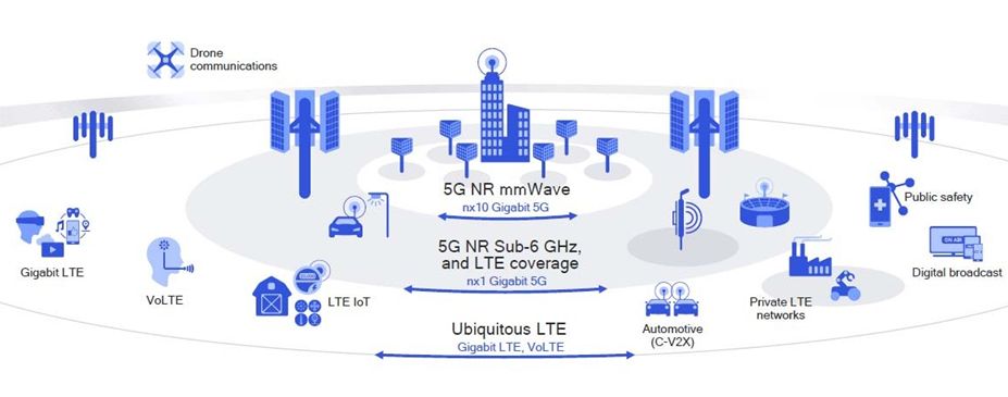
● 5G Base Stations: 5G communication has extremely high requirements for the stability and speed of signal transmission. The PCB with metal edging can provide excellent electromagnetic shielding for the radio - frequency modules and signal processing units in the base station, reducing electromagnetic interference between different modules and ensuring the stable transmission of millimeter - wave signals. Its outstanding heat - dissipation performance can effectively reduce the heat generated during the operation of the equipment, ensuring the long - term stable operation of 5G base stations and improving communication quality and efficiency.
● Satellite Communication Equipment: The satellite communication environment is complex, and signals are vulnerable to interference. The PCB with metal edging can not only enhance the mechanical strength of the equipment to adapt to the harsh space environment but also resist cosmic rays and various electromagnetic interferences through its electromagnetic shielding function, ensuring the accurate transmission of signals between satellites and ground stations and maintaining the stability of the communication link.
2.Automotive Electronics Field
● Autonomous Driving Systems: Sensors such as millimeter - wave radars, lidars, and vehicle - mounted cameras in autonomous vehicles have strict requirements for the reliability of signal processing and transmission. The PCB with metal edging can provide reliable electromagnetic shielding to prevent sensor signals from being interfered by other in - vehicle electronic devices, ensuring the accurate transmission of data. This helps the vehicle achieve precise environmental perception and decision - making control, enhancing the safety and reliability of autonomous driving.
● Battery Management Systems in New Energy Vehicles: The battery management system of new energy vehicles needs to monitor and control the battery status in real - time. The PCB with metal edging can provide good grounding and electromagnetic shielding for the battery management chips and circuits, avoiding signal interference. This ensures that the battery management system can accurately monitor parameters such as battery voltage, current, and temperature, guaranteeing the safe and efficient operation of the battery and extending its service life.
3.Aerospace Field
● Aircraft Navigation Systems: During flight, aircraft are affected by various factors such as strong vibrations and complex electromagnetic environments. The PCB with metal edging can enhance the structural strength of the navigation system, reducing the impact of vibrations on the circuit. At the same time, its electromagnetic shielding and heat - dissipation functions can ensure the stable operation of the navigation system, guaranteeing accurate aircraft navigation, avoiding flight deviations, and improving flight safety.
● Avionics Equipment: Avionics equipment on aircraft, such as communication, radar, and autonomous - driving systems, has extremely high requirements for the reliability of PCBs. The PCB with metal edging can provide good mechanical protection and electromagnetic shielding. In extreme environments such as high temperature, high pressure, and strong electromagnetic interference, it ensures the stable operation of the equipment and the successful completion of flight missions.
4.Medical Electronics Field
● Medical Imaging Equipment: Medical imaging equipment such as magnetic resonance imaging (MRI) and computed tomography (CT) has extremely high requirements for the stability and accuracy of signals. The PCB with metal edging can effectively shield external electromagnetic interference, ensuring that the imaging equipment can obtain high - resolution image data, which helps doctors make more accurate diagnoses.
● Life - Support Equipment: Life - support equipment such as pacemakers and ventilators is crucial for patients' lives. The PCB with metal edging can improve the anti - interference ability of the equipment, ensuring its stable operation and providing reliable life support for patients.
5.Industrial Control Field
● Automated Production Line Equipment: Equipment such as industrial robots and programmable logic controllers (PLCs) in automated production lines needs to operate accurately and stably in a complex electromagnetic environment. The PCB with metal edging can provide good electromagnetic shielding and mechanical strength, ensuring the reliability of the equipment in the industrial environment and improving production efficiency and product quality.
● Power Electronics Equipment: In high - voltage and high - current power electronics equipment, the PCB with metal edging can ensure the stable operation of the circuit through its good grounding and heat - dissipation performance, preventing equipment failures caused by overheating and electromagnetic interference and guaranteeing the safe and stable operation of the power system.