
0102030405


4-Layer Gold-Immersion High-Frequency Hybrid Multifunctional PCB | Advanced Circuit Solution


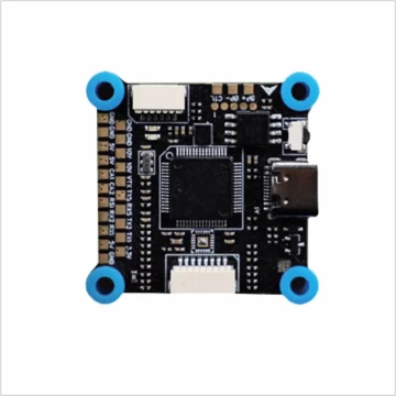
Product Details and Specifications

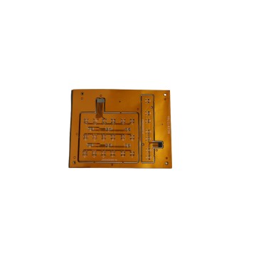
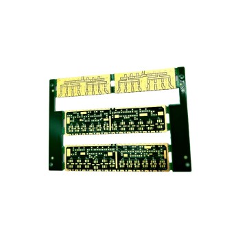
Our 4 - layer multifunctional PCB with gold - immersion through - holes and high - frequency hybrid design stands out for its innovative features and superior performance.
Type: High - frequency hybrid PCB | Gold - immersion through - hole PCB | Impedance - controlled PCB | Half - hole PCB | Multifunctional PCB
Material: High - frequency materials + FR - 4 TG170 RO4350B + IT180A
Number of Layers: 4L
PN: B0491495A
Manufacturing Highlights: Key Technologies in PCB Production
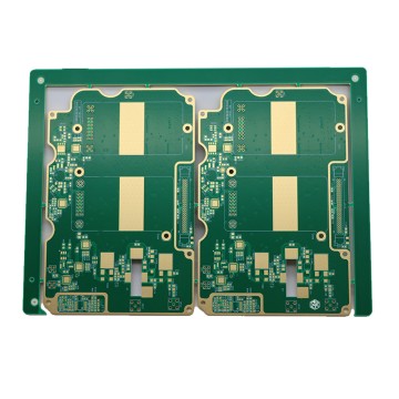
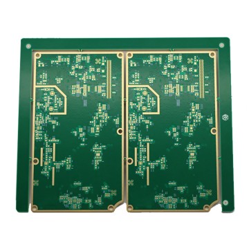
In the highly competitive PCB manufacturing landscape, our 4 - layer multifunctional PCBs represent the forefront of technological innovation. As an industry - leading PCB manufacturer, we combine the advantages of advanced materials and state - of - the - art processing techniques to achieve outstanding circuit board performance.
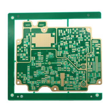
Key Manufacturing Features
Advanced Material Integration: The combination of FR - 4, TG170, RO4350B, and IT180A materials brings together the benefits of excellent electrical insulation, high - temperature resistance, low - loss in high - frequency applications, and enhanced mechanical properties. This integration allows the PCB to perform well in various operating conditions and meet the diverse requirements of different applications.
Gold - Immersion Through - Hole Technology: The gold - immersion through - hole process ensures low - resistance electrical connections, which is essential for high - speed signal transmission. It also provides a highly reliable connection interface for components, reducing the risk of connection failures and improving the overall reliability of the PCB.
High - Precision Impedance Control: Our advanced manufacturing processes enable precise impedance control, which is crucial for high - frequency and high - speed applications. By accurately controlling the impedance, we can minimize signal reflection and attenuation, ensuring stable and efficient signal transmission across the PCB.
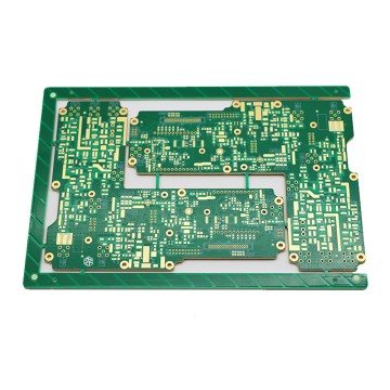
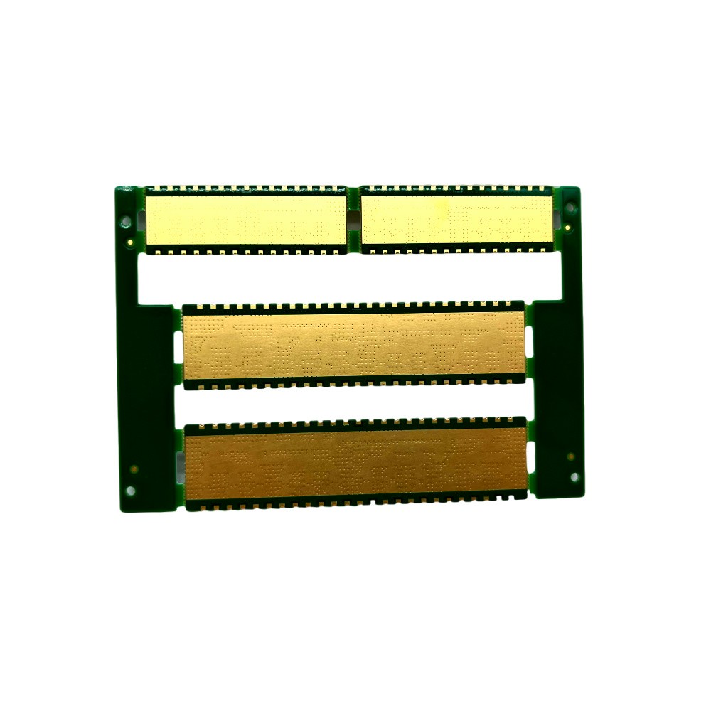
Half - Hole Technology: The half - hole design offers greater flexibility in PCB assembly. It allows for easier connection with other components or boards, simplifying the overall assembly process and enhancing the modularity of the electronic product. This technology is especially useful in applications where space is limited and complex connections are required.
Multi - Board Combination Design: The 4 - board combination design optimizes the functionality and space utilization of the PCB. It allows for the integration of multiple functions on a single PCB, reducing the overall size and weight of the electronic product while increasing its functionality and performance.
Essential Knowledge for PCB Design! How to Balance the Location, Layout of Half - holes and PCB Mechanical Strength?
1. Half hole design and layout
● How to plan the position of half holes reasonably based on circuit function and signal flow direction in PCB design? For example, in multi-layer PCBs, what are the effects of half hole positions on signal transmission between different layers?
When designing a PCB, to plan the positions of half - holes based on circuit functions and signal flow directions, it is necessary to first clarify the functions of different circuit modules and the signal transmission paths. For high - frequency signal circuits, the half - holes should be placed as close as possible to the signal source and the receiving end to shorten the signal transmission distance and reduce signal loss and interference. For example, in a radio - frequency circuit, placing the half - holes close to the radio - frequency chip and the antenna connection point can ensure efficient transmission of high - frequency signals.

In a multi - layer PCB, the position of the half - holes has a significant impact on inter - layer signal transmission. If the half - holes are located between signal layers and are in inappropriate positions, problems such as signal reflection and crosstalk may occur during inter - layer signal transmission. For example, when a half - hole is too close to a high - speed differential signal line, it will change the impedance characteristics of the differential line and cause signal distortion. Therefore, the relative positions of the half - holes and the signal layers should be reasonably planned, and a certain safe distance should be maintained to avoid adverse effects on inter - layer signal transmission.
When there are multiple types of half - holes on a PCB (such as half - holes for connecting different components) How to optimize their layout to reduce mutual interference?
When there are multiple types of half - holes on a PCB (such as half - holes for connecting different components), their layout can be optimized by grouping them according to the functions of the components and the types of signals. The half - holes connecting components of the same functional module should be placed together to reduce the crossing and proximity of half - holes in different groups. For example, the half - holes connecting components of the power module can be concentrated in the power area, and the half - holes connecting components of the communication module can be placed in the communication area.
At the same time, the spacing between the half - holes needs to be considered. Appropriate spacing should be set according to the characteristics of the signals and the degree of interference. For half - holes connected to sensitive signals, increase the spacing from other half - holes to prevent signal interference. The ground layer or shielding layer of the PCB can also be used to isolate different types of half - holes. For example, a ground layer can be set between two groups of half - holes to block the mutual coupling of signals.
What impact does the layout of half holes have on the mechanical strength of PCBs? How to balance the relationship between half hole layout and overall mechanical strength of PCB during design?
The layout of half - holes will weaken the mechanical strength of the PCB. Since half - holes damage the overall structural integrity of the PCB, especially when there are a large number of half - holes and they are concentrated, the mechanical strength of that area will be significantly reduced. When subjected to external forces, problems such as cracking and delamination are likely to occur.
When designing, it is necessary to balance the relationship between the layout of half - holes and the overall mechanical strength of the PCB. First, try to avoid densely arranging half - holes at the edges or stress - concentrated areas of the PCB. If half - holes must be set in these areas, the mechanical strength can be increased by adding auxiliary support structures or stiffeners. Second, distribute the half - holes reasonably to avoid over - concentration of half - holes in local areas. For example, adopt a dispersed layout to evenly distribute the impact of half - holes on the mechanical strength of the PCB. In addition, perform mechanical strength simulation analysis in the PCB design software, and adjust the layout of half - holes according to the analysis results to ensure that the PCB has sufficient mechanical strength while meeting the circuit functions.
How to Determine the Aperture Detection, Non - destructive Testing, and Sampling Inspection Plans for PCB Half - hole Quality Inspection?

Currently, there are various methods available for detecting the quality of half - holes. For aperture detection, the commonly used method is the optical measurement method. By measuring the magnified image of the half - hole through an optical microscope or an electron microscope, the aperture size can be accurately obtained. There is also the laser measurement method, which uses the reflection principle of laser to measure the aperture quickly and non - contactly, with high precision. When it comes to detecting the integrity of the hole wall, the microscope observation method can directly check whether there are defects such as cracks and delamination on the hole wall. The ultrasonic detection method is also very effective. It emits ultrasonic waves and judges the internal structural integrity of the hole wall based on the situation of the reflected waves. When detecting the reliability of the connection between the half - hole and the circuit, the flying probe test can conduct electrical performance tests on the connection between a single half - hole and the circuit to check for problems such as open circuits and short circuits. ICT (In - Circuit Test) can comprehensively detect the connection reliability of half - holes in the entire circuit system after the circuit board is assembled.
For the non - destructive testing of the quality of internal half - holes in multi - layer PCBs, X - ray detection technology can be used. X - rays can penetrate the multi - layer structure of the PCB, and through imaging, the shape, position of the internal half - holes and their connection with the surrounding circuits can be clearly shown, and defects such as misalignment and voids can be detected. There is also micro - focus CT testing, which can perform tomographic scanning on the PCB to generate 3D images of the internal half - holes, allowing for a more comprehensive observation of the quality of the half - holes, including minor defects in the hole wall and changes in the aperture. In addition, acoustic microscope testing is also suitable for the quality inspection of internal half - holes in multi - layer PCBs. It uses the propagation characteristics of sound waves in different media and analyzes the reflected waves to judge the quality of the half - holes, and is particularly effective in detecting defects such as delamination.
How to develop a reasonable half hole quality inspection plan in mass production that can ensure product quality and improve production efficiency?
In mass production, when formulating a reasonable sampling inspection plan for the quality of half - holes, first, the sampling inspection ratio needs to be determined. For production batches with high quality stability, the sampling inspection ratio can be appropriately reduced; for new batches or batches with unstable quality, the sampling inspection ratio should be increased. For example, a sampling inspection ratio of 5% - 10% can be used for new batches, and 2% - 5% for stable batches. Secondly, the stratified sampling method is adopted. Products are stratified according to factors such as different production time periods and production equipment, and then samples are randomly selected from each layer for testing to ensure that products from all production links are covered. Furthermore, set key quality control points, such as conducting a sampling inspection after a certain number of products are produced, or conducting a sampling inspection after changing the production raw materials. During the inspection process, if a serious quality problem is found in a certain sample, the sampling inspection intensity should be immediately increased, and more products should be inspected to ensure the quality of the entire batch of products. In this way, product quality can be ensured while improving production efficiency.
Versatile Applications of Our High - Performance PCBs
Our 4 - layer high - frequency hybrid and multifun ctional PCBs are designed to meet the demands of various industries that require reliable and high - performance circuit boards. Here are some of the key application areas:
1.5G Communication
● Description: The PCB is ideal for 5G base stations, RF modules, and antennas, ensuring high-speed data transmission with minimal signal loss.
● Benefits: Supports the growing demand for faster and more reliable wireless communication networks.
2.Aerospace Electronics
● Description: Used in avionics, satellite communication, and radar systems, where reliability and performance are critical.
● Benefits: Ensures stable operation in extreme conditions, such as high altitude and temperature fluctuations.
3.Medical Devices
● Description: Applied in MRI machines, CT scanners, and patient monitoring systems, where precision and reliability are paramount.
● Benefits: Enhances the accuracy and performance of medical diagnostics and treatments.
4.Industrial Automation
● Description: Used in PLCs, motor drives, and control panels for efficient and reliable operation in industrial settings.
● Benefits: Improves productivity and reduces downtime in manufacturing processes.
5.Automotive Electronics
● Description: Integrated into ADAS, infotainment systems, and engine control units, ensuring safety and connectivity in modern vehicles.
● Benefits: Enhances the performance and reliability of automotive electronics.
6.High-Speed Computing
● Description: Supports servers, data centers, and AI accelerators, enabling fast data processing and efficient operation.
● Benefits: Ensures high performance in data-intensive environments.
7.IoT Devices
● Description: Used in smart sensors and edge computing devices, enabling seamless connectivity and data processing.
● Benefits: Supports the growth of smart solutions in various industries.
8.Energy Management
● Description: Applied in smart grid systems and energy storage controllers, ensuring efficient power distribution and monitoring.
● Benefits: Enhances the reliability and efficiency of energy management systems.
9.Military and Defense
● Description: Used in communication systems and electronic warfare, ensuring reliable performance in mission-critical operations.
● Benefits: Provides robust solutions for defense applications.
10.Consumer Electronics
● Description: Integrated into smartphones, tablets, and wearables, enhancing functionality and user experience.
● Benefits: Ensures high performance and reliability in compact and portable devices.
Our 4-layer gold-immersion through-hole high-frequency hybrid multifunctional PCB is a cutting-edge solution designed to meet the demands of advanced electronic applications. With its precise impedance control, gold-immersion through-holes, and high-frequency hybrid design, this PCB delivers unmatched performance and reliability. Whether you're developing 5G communication systems, aerospace electronics, or medical devices, our PCB provides a solid foundation for high-performance products. Backed by rigorous testing and comprehensive support, we are your trusted partner for innovative PCB solutions.