








0102030405
PCB Knowledge
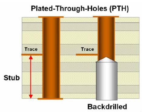
Analysis of Back Drilling Technology in High Speed PCB Design
2020-04-08
The PCB via is usually designed as through-holes (from the top surface to the bottom layer). When the PCB line connecting the via is routed closer to the top layer, a “stub”bifurcation will occur at the via of the PCB interconnect link