








RF PCB Temperature Compensation: Hybrid Stack-Up Strategy with Negative and Positive TCDk Materials
1. The Temperature Problem That Won't Go Away
A power amplifier tuned to perfection at 25°C drifts off frequency at 85°C. A 5G beamforming antenna that delivers precise phase alignment at room temperature produces grating lobes in the summer heat. A millimeter-wave radar module that passes factory test fails field validation because the PCB heated up during operation.
The culprit is almost always the same: the dielectric constant (Dk) of the PCB substrate changed with temperature.
Dk determines the propagation velocity of signals in a PCB. When Dk changes, impedance shifts, phase angles rotate, and resonant frequencies drift. For RF and microwave circuits operating above 10 GHz, even a small Dk shift can push a filter out of band, degrade return loss by several dB, or introduce phase errors that destroy beamforming accuracy.
The standard industry response has been to select materials with low TCDk (temperature coefficient of dielectric constant) — materials whose Dk changes minimally with temperature. Rogers RO3003, with a TCDk of only -3 ppm/°C, is a prime example.
But low TCDk alone is not always sufficient. For wide-temperature-range applications — automotive (-40°C to +125°C), aerospace (-55°C to +125°C), or high-power RF (+85°C to +150°C) — the cumulative Dk shift, even from a low-TCDk material, can be significant.
This is where hybrid stack-up temperature compensation enters the picture. By combining materials with opposing TCDk signs — negative coefficient materials and positive coefficient materials — in a single PCB stack-up, designers can cancel Dk drift across temperature, achieving effective temperature compensation without compromising RF performance.
2. Understanding TCDk: The Language of Temperature Drift
2.1 What Is TCDk?
TCDk (Temperature Coefficient of Dielectric Constant) quantifies how much a material's Dk changes per degree Celsius of temperature change. It is expressed in ppm/°C (parts per million per degree Celsius).
The formula is:
TCDk = [Dk(T₂) - Dk(T₁)] / [Dk(T₁) × (T₂ - T₁)]
A negative TCDk means Dk decreases as temperature rises. A positive TCDk means Dk increases as temperature rises.
2.2 The Impact on RF Performance
When Dk changes with temperature, several critical RF parameters shift:
Impedance: Characteristic impedance is inversely proportional to the square root of Dk. A Dk increase lowers impedance; a Dk decrease raises impedance.
Phase: Signal phase is proportional to the square root of Dk multiplied by path length. A Dk change of 1% creates a phase error of approximately 0.5% — significant in phased array applications.
Resonant frequency: Resonant frequency is inversely proportional to the square root of Dk. A 1% Dk increase lowers resonant frequency by approximately 0.5%.
Propagation delay: Signal velocity decreases as Dk increases, adding timing skew to high-speed digital interfaces.
For a 77 GHz automotive radar operating from -40°C to +125°C, a material with TCDk of -50 ppm/°C experiences a Dk shift of approximately -0.8% over the temperature range — enough to shift the radar's resonant frequency by 400 MHz or more.
2.3 The TCDk Spectrum of Common Materials
Table 1 — TCDk of common PCB materials
| Material | Typical Dk | TCDk (ppm/°C) | TCDk Sign | Application |
|---|---|---|---|---|
| Rogers RO3003 | 3.00 | -3 | Negative | Millimeter-wave, radar |
| Rogers RO4835 | 3.48 | +50 | Positive | 5G, microwave |
| Rogers RT/duroid 5880 | 2.20 | -125 | Negative | High-frequency, low-loss |
| Taconic RF-35 | 3.50 | -150 | Negative | General RF |
| FR-4 (standard) | 4.2-4.8 | -200 to -400 | Negative | Low-frequency, cost-sensitive |
| PTFE (unfilled) | 2.1 | ~0 to -50 | Negative/Neutral | Ultra-low loss |
| LCP | 3.0-3.5 | ±20 | Variable | Millimeter-wave, flexible |
The key observation: most PCB materials have negative TCDk — Dk decreases as temperature rises. Materials with positive TCDk are rarer but exist, notably Rogers RO4835 with +50 ppm/°C and certain ceramic-filled PTFE formulations.
This is the foundation of the hybrid compensation strategy.
3. The Hybrid Compensation Principle: Opposites Cancel
3.1 The Core Idea
If a negative-TCDk material decreases Dk with temperature, and a positive-TCDk material increases Dk with temperature, then combining them in a single stack-up can produce net-zero Dk drift — or at least, significantly reduced drift.
The compensation works because the signal's electromagnetic field does not reside entirely in a single dielectric layer. In a microstrip or stripline structure, the field distributes across multiple dielectric layers. By placing a positive-TCDk layer adjacent to a negative-TCDk layer, the Dk shift of one layer offsets the Dk shift of the other.
The effective TCDk of the composite stack-up is the weighted average of the individual layer TCDks, weighted by the fraction of the total electromagnetic field energy contained in each layer.
3.2 A Practical Example: RO3003 + RO4835 Hybrid
Consider a hybrid stack-up combining:
• RO3003 (negative TCDk: -3 ppm/°C)
• RO4835 (positive TCDk: +50 ppm/°C)
RO3003 provides ultra-low TCDk for the critical RF signal layer — its Dk is nearly flat across temperature. RO4835, with its positive TCDk, can be placed in adjacent layers to provide a slight upward Dk trend that offsets any residual negative drift from other materials in the stack-up.
This combination is particularly attractive because both materials are from Rogers' hydrocarbon-ceramic family and process similarly to FR-4, simplifying manufacturing.
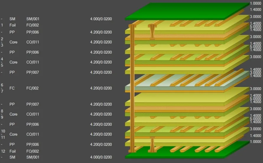
3.3 Stack-Up Configurations for Temperature Compensation
Configuration A — Microstrip with compensation layer:
Layer: Signal — Material: RO3003 — TCDk: -3 ppm/°C — Function: Critical RF traces
Layer: Dielectric — Material: RO4835 prepreg — TCDk: +50 ppm/°C — Function: Compensation + bonding
Layer: Ground — Material: Copper — TCDk: — Function: Reference plane
The signal field extends into both the RO3003 and the RO4835. The positive TCDk of the RO4835 partially cancels the negative drift of the RO3003 (and any temperature-dependent effects in the copper).
Configuration B — Stripline with balanced compensation:
Layer: Ground — Material: Copper — TCDk: — Function: Reference
Layer: Dielectric 1 — Material: RO4835 — TCDk: +50 ppm/°C — Function: Upper compensation
Layer: Signal — Material: RO3003 — TCDk: -3 ppm/°C — Function: Buried RF traces
Layer: Dielectric 2 — Material: RO4835 — TCDk: +50 ppm/°C — Function: Lower compensation
Layer: Ground — Material: Copper — TCDk: — Function: Reference
With symmetric compensation layers above and below the signal, the temperature compensation is balanced, and the stack-up remains mechanically stable.
3.4 The Role of Prepreg in Hybrid Compensation
Prepreg materials play a critical role in hybrid temperature compensation. The prepreg bonding layers between cores contribute to the overall Dk and TCDk of the stack-up.
RO4450F, a commonly used prepreg for bonding Rogers materials, has a Dk of approximately 3.52 and a TCDk that must be accounted for in the composite calculation. In a hybrid stack-up, the prepreg's TCDk contribution can either reinforce or oppose the compensation effect — a detail that must be modeled carefully in electromagnetic simulations.
4. Why Not Just Use Low-TCDk Materials Exclusively?
If low TCDk is the goal, why not use RO3003 (TCDk = -3 ppm/°C) for every layer and call it done?
Cost: RO3003 and other high-performance RF materials are significantly more expensive than FR-4. An all-RO3003 board can cost 5-10× more than a hybrid design that uses RO3003 only on critical RF layers.
Mechanical properties: High-frequency materials may have different CTE (coefficient of thermal expansion) than standard materials, creating warpage and reliability risks in large panels.
Availability: Some high-frequency materials have longer lead times or limited availability.
The hybrid approach — using low-TCDk materials only where needed, and using positive-TCDk or standard materials elsewhere — achieves temperature compensation at a fraction of the cost of an all-high-performance design.
Table 2 — Temperature compensation strategies compared
| Strategy | Cost | Temperature Stability | Manufacturing Complexity | Best For |
|---|---|---|---|---|
| Single low-TCDk material (e.g., RO3003) | High | Excellent (TCDk = -3) | Low | Ultra-high precision, millimeter-wave |
| Hybrid: low-TCDk RF layers + FR-4 support | Moderate | Good | Moderate | Cost-sensitive RF applications |
| Hybrid: negative + positive TCDk compensation | Moderate-High | Excellent (net-zero drift) | High | Wide temperature range, high stability |
5. Design Considerations for Hybrid Temperature Compensation
5.1 Field Distribution Analysis
The effectiveness of hybrid temperature compensation depends on the fraction of the electromagnetic field that resides in each dielectric layer. In microstrip, approximately 60-70% of the field is in the substrate immediately beneath the signal trace; the remainder is in the air above and in deeper layers.
For compensation to work, the positive-TCDk material must be placed where the field has significant energy — typically within 2-3 substrate thicknesses of the signal layer. Placing the compensation layer too far from the signal reduces its effectiveness.
5.2 CTE Matching
Hybrid stack-ups combine materials with different CTEs. If the CTE mismatch is too large, thermal cycling can cause delamination, warpage, or plated through-hole cracking.
RO3003 has X/Y CTE of approximately 17/16 ppm/°C, while RO4835 has X/Y CTE of approximately 10/12 ppm/°C. This difference is manageable with proper lamination control, but it must be considered in the stack-up design.
5.3 Lamination Process Control
Hybrid stack-ups require precise lamination control. The different materials may have different curing temperatures, resin flow characteristics, and shrinkage rates.
Key considerations:
• Limit total lamination cycles to prevent Dk drift
• Use low-flow prepregs to control resin bleed into the flex area
• Validate Dk/Df stability under actual temperature conditions
• Conduct cross-section and impedance analysis on pilot runs
5.4 Simulation and Modeling
Standard impedance calculators that assume a single dielectric material cannot accurately model hybrid stack-ups.
For hybrid temperature compensation designs:
• Use full-wave 3D electromagnetic simulation (HFSS, CST) that models each dielectric layer separately
• Include temperature-dependent Dk in the material models
• Validate simulation results with TDR impedance measurements on test coupons
6. Summary: The Compensation Strategy for Temperature-Stable RF
Temperature-induced Dk drift is a fundamental challenge in RF PCB design. The traditional approach — selecting materials with the lowest possible TCDk — works but is expensive and may not achieve the stability required for wide-temperature-range applications.
Hybrid stack-up temperature compensation offers an alternative: combining materials with opposing TCDk signs to cancel Dk drift across temperature.
The key takeaways:
• Most PCB materials have negative TCDk — Dk decreases as temperature rises
• Positive TCDk materials (e.g., RO4835 at +50 ppm/°C) are available and can offset negative drift
• Hybrid stack-ups combine negative and positive TCDk materials to achieve net-zero Dk drift
• RO3003 + RO4835 is a practical combination: ultra-low TCDk signal layer + positive-TCDk compensation layer
• The compensation effect depends on field distribution — place compensation layers where the signal field has significant energy
• CTE matching and lamination control are critical for hybrid stack-up reliability
• Full-wave simulation is required to accurately model hybrid stack-ups
A well-designed hybrid stack-up with temperature compensation achieves the phase stability, impedance consistency, and frequency accuracy that RF systems demand — without the cost of an all-high-performance-material board. The compensation is not in the circuit. It is in the stack-up.
7. Frequently Asked Questions:
Q1: What is TCDk and why does it matter for RF PCBs?
A: TCDk (Temperature Coefficient of Dielectric Constant) measures how much a material's Dk changes per degree Celsius. It matters because Dk changes shift impedance, phase, and resonant frequency — degrading RF performance. A negative TCDk means Dk decreases as temperature rises.
Q2: What is the TCDk of Rogers RO3003?
A: Rogers RO3003 has a TCDk of approximately -3 ppm/°C from -50°C to 150°C — one of the lowest TCDk values available, making it nearly temperature-stable.
Q3: What materials have positive TCDk?
A: Rogers RO4835 has a positive TCDk of +50 ppm/°C. Some TC Series materials from Rogers have TCDk values ranging from -9 to -75 ppm/°C, with certain formulations approaching positive values.
Q4: How does hybrid stack-up temperature compensation work?
A: By combining negative-TCDk and positive-TCDk materials in a single stack-up, the Dk drift of one layer offsets the drift of the other. The effective TCDk of the composite is the weighted average of the individual layer TCDks.
Q5: Why not just use RO3003 for every layer?
A: Cost. RO3003 and other high-performance RF materials are significantly more expensive than FR-4 or standard materials. A hybrid approach uses low-TCDk materials only on critical RF layers, with lower-cost materials elsewhere.
Q6: What is a practical hybrid compensation stack-up example?
A: Use RO3003 (TCDk = -3 ppm/°C) for the RF signal layer and RO4835 (TCDk = +50 ppm/°C) for adjacent dielectric layers. The positive TCDk of RO4835 offsets any residual negative drift, achieving near-zero composite TCDk.
Q7: Does the compensation layer need to be close to the signal layer?
A: Yes. The compensation effect depends on the fraction of the electromagnetic field that resides in each dielectric layer. The compensation layer should be within 2-3 substrate thicknesses of the signal layer for maximum effectiveness.
Q8: What are the manufacturing challenges of hybrid stack-ups?
A: CTE mismatch between different materials can cause warpage or delamination. Different curing temperatures and resin flow characteristics require precise lamination control. Full-wave simulation is needed to accurately model the stack-up.
Q9: Can FR-4 be used in a temperature-compensated hybrid stack-up?
A: Yes, but FR-4 has a large negative TCDk (-200 to -400 ppm/°C) and high loss, making it unsuitable for RF signal layers. FR-4 can be used for non-critical layers (power, control, ground) while high-performance materials handle the RF layers.
Q10: How do I verify temperature compensation in my design?
A: Include impedance coupons on the production panel and measure them at multiple temperatures (e.g., -40°C, 25°C, 85°C, 125°C). Compare measured impedance and phase against simulation. Validate Dk/Df stability under actual temperature conditions.
8. About Richfulljoy
Richfulljoy specializes in high-performance RF and microwave PCB manufacturing with advanced hybrid stack-up capabilities for temperature compensation. Our engineering team understands that Dk temperature stability is a first-order RF performance parameter — and we apply the right material combinations to achieve it.









