











Rigid-Flex Coverlay Opening Copper Protection: ENIG Thickness Requires Special Control
1. The Exposed Copper Problem
In a rigid-flex PCB, the coverlay — a laminated polyimide film with adhesive — protects the copper traces in the flex area from oxidation, mechanical wear, and environmental damage. Where components must be soldered or connections made, openings are created in the coverlay to expose the copper pads beneath.
These exposed copper pads must be protected with a surface finish. Electroless nickel / immersion gold (ENIG) is the most common choice for rigid-flex PCBs because it provides excellent solderability, flatness for fine-pitch components, and corrosion resistance. The ENIG process deposits a nickel barrier layer (typically 3–6μm) followed by a thin immersion gold layer (0.05–0.10μm).
However, at coverlay openings in the flex area — where the copper is exposed and the board must bend — ENIG thickness requires special control. The nickel layer is inherently brittle. When a flex circuit bends, nickel cracks more readily than copper. These cracks can propagate through the copper beneath, leading to trace failure.
This article explains why standard ENIG thickness specifications for rigid boards are inadequate for coverlay openings in flex areas, what special controls are required, and how to specify ENIG for reliable rigid-flex PCB performance.
2. Coverlay Openings: Where Copper Is Most Vulnerable
2.1 What Is a Coverlay Opening?
A coverlay opening is the exposed area in the polyimide coverlay layer that allows access to copper pads for soldering, bonding, or electrical connection. Unlike liquid solder mask on rigid boards — which is imaged after lamination — coverlay openings are created by mechanical punching, routing, or laser cutting before lamination. The coverlay is then laminated under heat and pressure.
This pre-lamination process introduces dimensional variation. In volume production, coverlay opening tolerance is typically controlled within ±50–100μm, depending on the cutting method, panel stability, and lamination conditions. Material shrinkage, adhesive flow, and panel distortion during lamination affect the final opening size and position.
2.2 The Copper Exposure Risk
When a coverlay opening is too large, unsupported copper becomes exposed near a bend and starts a crack path. When the opening is too small, adhesive can creep onto the pad and weaken solder wetting.
For the exposed copper at coverlay openings, ENIG provides the protective barrier. But ENIG — specifically the nickel layer — behaves differently on a flex circuit than on a rigid board. The nickel adds stiffness to the exposed pad. In a bend zone, that stiffness becomes a liability.
2.3 Why the Flex Area Is Different
In rigid areas, ENIG nickel thickness can follow the standard IPC-4552 specification of 3–6μm. The nickel provides a reliable diffusion barrier and solderable surface. There is no bending stress, so nickel brittleness is not a concern.
In the flex area — particularly at coverlay openings — the situation is fundamentally different. The flex circuit bends. The copper traces and pads experience tensile and compressive strain. The ENIG nickel layer, being brittle, cannot accommodate this strain. It cracks. Those cracks propagate through the copper beneath.
At a coverlay opening, the problem is amplified. The coverlay edge creates a stress concentration point. The exposed copper pad is unsupported by coverlay on one side. When the flex bends, the strain concentrates at the coverlay edge — exactly where the ENIG-plated copper is exposed.
3. Why Standard ENIG Thickness Fails in Flex Areas
3.1 The Nickel Brittleness Problem
Nickel is fundamentally brittle compared to copper. It does not fare well when flexed. The typical result of bending a nickel-plated trace or contact is that the nickel develops cracks, and those cracks propagate through the copper below.
The ENIG nickel layer is typically 3–6μm thick — a substantial layer relative to the thin copper traces (12–35μm) used in flex circuits. When the flex bends, the nickel layer cannot deform plastically like copper. It fractures. Once the nickel cracks, the crack tip concentrates stress into the copper beneath, accelerating copper fatigue failure.
Table 1 — ENIG nickel thickness and flex cracking risk
| Nickel Thickness | Flex Cracking Risk | Typical Application |
|---|---|---|
| <2μm | Low (thin nickel cracks less) | Not recommended — black pad risk |
| 2–3μm | Moderate | Some flex applications with high-P nickel |
| 3–6μm (IPC-4552 standard) | High | Rigid boards only — not for flex bend zones |
| >6μm | Very high | Never use in flex areas |
3.2 The Thickness Dilemma
The PCB industry faces a dilemma with ENIG on flex circuits. IPC-4552 specifies 3–6μm nickel for rigid boards. If you apply this same specification to a flex circuit, the nickel is thick enough to crack during bending.
If you reduce the nickel thickness to overcome brittleness, you open yourself to "black pad" failures — excessive corrosion of the nickel layer during the immersion gold step, creating a brittle, non-wettable surface.

3.3 The Coverlay Opening Amplification
At a coverlay opening, the cracking problem is worse for three reasons:
Stress concentration at the coverlay edge. The coverlay edge creates a mechanical discontinuity. When the flex bends, strain concentrates at this edge. The ENIG-plated copper pad is most vulnerable exactly where the coverlay ends.
Exposed pad geometry. Coverlay openings are typically larger than the pad itself to accommodate registration tolerance. A common rule is pad + 0.10–0.15mm per side. This means the copper pad extends beyond the coverlay edge — unsupported copper that must bear the full bending strain.
Adhesive flow. During lamination, adhesive can flow into the coverlay opening, reducing the effective opening size. This can create uneven stress distribution on the exposed pad, accelerating crack initiation at the points where adhesive meets the pad edge.
3.4 Testing Evidence
Bending tests on flexible substrates have quantified the impact of nickel thickness. When flexible substrates were plated with nickel to 2μm and 5μm thicknesses, the 2μm samples did not crack during bending, while the 5μm samples developed cracks.
The difference is dramatic: a 5μm nickel layer — well within the IPC-4552 standard — cracks under flexure. A 2μm nickel layer survives the same bending stress. Yet reducing nickel thickness below 3μm introduces black pad risk.
The solution is not simply to reduce thickness. It is to change the nickel chemistry.
4. The Solution: High-Phosphorus ENIG for Flex Areas
4.1 Phosphorus Content and Ductility
The brittleness of electroless nickel depends on its phosphorus content. Standard ENIG uses medium-phosphorus nickel (7–9% phosphorus by weight). This medium-P nickel is harder and more brittle.
High-phosphorus nickel (10–13% phosphorus by weight) has different mechanical properties. It is more ductile — it can accommodate bending strain without cracking. The increased phosphorus content changes the crystal structure and grain structure of the nickel deposit, reducing internal stress and increasing flexibility.
The ENIG process with high-phosphorus nickel offers a more reliable surface finish for flex and rigid-flex applications. High-phosphorus ENIG provides the corrosion resistance and solderability of standard ENIG while surviving the mechanical demands of dynamic bending.
4.2 High-P ENIG at Coverlay Openings
For coverlay openings in flex areas, high-phosphorus ENIG is the recommended solution. It allows the nickel layer to bend without cracking, protecting the copper beneath.
However, high-P ENIG has a limitation: it typically limits gold thickness to approximately 0.05μm. This is thinner than the 0.05–0.10μm gold layer used on rigid boards. The thinner gold is still sufficient to protect the nickel from oxidation during storage, but it requires tighter process control.
Thickness measurements in this range are challenging — equipment accuracy is approximately ±0.01μm. This means ENIG thickness specifications for flex areas must account for measurement uncertainty.
4.3 ENEPIG as an Alternative
For applications requiring thicker gold or wire bonding capability, ENEPIG (electroless nickel / electroless palladium / immersion gold) is an alternative. The palladium layer between nickel and gold provides additional corrosion protection and enables wire bonding.
However, ENEPIG still contains a nickel layer and is not suitable for highly dynamic flexing areas. The nickel brittleness problem remains. For coverlay openings in dynamic bend zones, high-phosphorus ENIG with controlled thin nickel is the preferred solution.
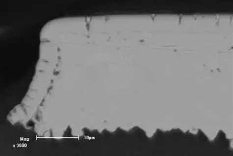
5. Design Guidelines for ENIG at Coverlay Openings
5.1 Specify High-Phosphorus ENIG
For any rigid-flex PCB with coverlay openings in the flex area — particularly in dynamic bending applications — specify high-phosphorus ENIG (10–13% P) rather than standard medium-P ENIG (7–9% P).
Fabrication note example:
"Surface finish: ENIG (electroless nickel / immersion gold) with high-phosphorus electroless nickel (10–13% P by weight). Nickel thickness: 2.5–3.5μm. Gold thickness: 0.04–0.06μm. Per IPC-4552 with flex-area modification."
5.2 Control Nickel Thickness
Reduce nickel thickness in the flex area. While IPC-4552 specifies 3–6μm for rigid boards, flex areas require thinner nickel — ideally 2.5–3.5μm.
Key points:
• Minimum nickel thickness: 2.5μm (to avoid black pad risk)
• Maximum nickel thickness: 3.5μm (to avoid cracking)
• Target: 3.0μm ±0.5μm
5.3 Coverlay Opening Design
Proper coverlay opening design reduces stress on the ENIG-plated pads.
Opening clearance: Use pad + 0.10–0.15mm per side for most SMT pads. For fine-pitch components, use pad + 0.075–0.125mm per side. Avoid overly large openings that leave unsupported copper.
Coverlay edge placement: Keep coverlay edges away from dynamic bend peaks. The coverlay opening should not be located at the maximum bend point.
Adhesive flow consideration: Account for adhesive flow during lamination, which can reduce effective opening size by 20–40μm per side. Specify opening dimensions that allow for this shrinkage while still providing adequate pad exposure.
Table 2 — Recommended ENIG specifications for coverlay openings by application
| Application Type | Nickel Type | Nickel Thickness | Gold Thickness | Rationale |
|---|---|---|---|---|
| Static flex (bend-to-install) | Medium-P or High-P | 3–4μm | 0.05–0.08μm | Limited bending — standard ENIG acceptable |
| Dynamic flex (<50,000 cycles) | High-P (10–13%) | 2.5–3.5μm | 0.04–0.06μm | Moderate bending — high-P nickel required |
| Dynamic flex (>50,000 cycles) | High-P (10–13%) | 2.5–3.0μm | 0.04–0.05μm | High-cycle bending — minimize nickel thickness |
| ZIF connector contacts | High-P or hard gold | 2.5–3.5μm | 0.04–0.06μm | Wear resistance — consider hard gold for >100 insertions |
5.4 Process Control Requirements
ENIG on flex circuits requires tighter process control than ENIG on rigid boards.
Nickel bath control: Monitor phosphorus content closely. High-P nickel baths require specific chemistry control to achieve 10–13% P content.
Gold bath control: Control immersion gold thickness to the lower end of the range (0.04–0.06μm) to avoid excessive gold that can embrittle solder joints.
Measurement: Use X-ray fluorescence (XRF) with appropriate calibration for thin coatings on flexible substrates. Account for measurement uncertainty of approximately ±0.01μm.
Testing: Perform bend testing on ENIG-plated coupons to verify that the nickel does not crack under the specified bend radius and cycle count.
6. Special Control for a Special Problem
ENIG at coverlay openings in rigid-flex PCBs requires special thickness control because the flex area subjects the brittle nickel layer to bending stress that does not exist in rigid boards.
The key takeaways:
• Nickel is brittle and cracks when flexed
• Standard ENIG (3–6μm nickel) cracks under bending
• Reducing nickel thickness below 3μm risks black pad failures
• High-phosphorus nickel (10–13% P) provides ductility without sacrificing corrosion resistance
• Target nickel thickness: 2.5–3.5μm for flex areas
• Target gold thickness: 0.04–0.06μm for flex areas
• Coverlay opening design must account for registration tolerance, adhesive flow, and stress concentration at the coverlay edge
A rigid-flex PCB with properly specified ENIG — high-phosphorus nickel at controlled thickness — will survive dynamic bending without cracking at the coverlay openings. A board that applies standard rigid-board ENIG specifications to the flex area will fail, often invisibly, at the coverlay edges.
The difference is not in the material cost. It is in the specification.
7. Frequently Asked Questions
Q1: Why is ENIG thickness a concern at coverlay openings in rigid-flex PCBs?
A: The ENIG nickel layer is brittle. At coverlay openings in the flex area, the exposed copper pads must bend. The nickel cracks under bending stress, and those cracks propagate through the copper beneath, causing trace failure.
Q2: What ENIG nickel thickness does IPC-4552 specify?
A: IPC-4552 specifies electroless nickel thickness of 3–6μm for rigid printed boards. This standard was developed for rigid boards, not for flex areas that must bend.
Q3: What happens if I use standard IPC-4552 ENIG on a flex area?
A: The 3–6μm nickel layer is thick enough to crack during bending. Bending tests show that 5μm nickel cracks while 2μm nickel does not. The cracks propagate through the copper beneath.
Q4: What is the solution to the nickel cracking problem?
A: Use high-phosphorus ENIG (10–13% phosphorus by weight) instead of standard medium-P ENIG (7–9% P). High-P nickel is more ductile and can accommodate bending strain without cracking.
Q5: What nickel thickness should I specify for coverlay openings in flex areas?
A: Target 2.5–3.5μm nickel thickness for flex areas. This is thinner than the IPC-4552 standard but sufficient to avoid black pad issues while minimizing cracking risk.
Q6: What gold thickness should I specify for flex area ENIG?
A: Target 0.04–0.06μm gold thickness. High-phosphorus ENIG typically limits gold thickness to approximately 0.05μm. The thinner gold still protects the nickel from oxidation.
Q7: What is black pad and why does it matter for flex ENIG?
A: Black pad is a defect where excessive corrosion of the nickel layer during the immersion gold step creates a brittle, non-wettable surface. If nickel thickness is reduced too much to avoid cracking, black pad risk increases.
Q8: How does coverlay opening design affect ENIG reliability?
A: Coverlay openings create stress concentration points at the coverlay edge. If the opening is too large, unsupported copper is exposed. If too small, adhesive creeps onto the pad. Proper opening clearance (pad + 0.10–0.15mm per side) is essential.
Q9: Can I use ENEPIG instead of ENIG for flex areas?
A: ENEPIG (ENIG with a palladium layer) offers better wire bonding capability. However, it still contains a nickel layer and is not suitable for highly dynamic flexing areas.
Q10: How do I specify ENIG for coverlay openings on my fabrication drawing?
A: Include a fabrication note: "Surface finish: ENIG with high-phosphorus electroless nickel (10–13% P). Nickel thickness: 2.5–3.5μm. Gold thickness: 0.04–0.06μm. Per IPC-4552 with flex-area modification. Bend test verification required."
8. About Richfulljoy
Richfulljoy specializes in high-reliability rigid-flex PCB manufacturing with advanced ENIG capabilities for flex areas. Our engineering team understands that ENIG thickness at coverlay openings requires special control — and we apply the right specifications to every flex design.
- Rigid-Flex PCB Lamination: Transition Slope Design for Rigid-Flex Thickness Differences
- Copper Grain Direction vs, Bending Axis; The First Principle Determining Dynamic Flex Life of Riaid-Flex PCBs
- Rigid-Flex PCB Bend Radius Limits: Dynamic vs Static Flex Life Differs by an Order of Magnitude
- Rigid-Flex Flex Area Routing: How Arc vs. 45° Corners Impact Dynamic Bend Life
- Rigid-Flex PCB Electromagnetic Shielding: Flex Area Shield Layer Design — Critical Considerations Often Overlooked
- Rigid-Flex PCB CAF Risk: CAF Pathways in the Flex Area Are Different from Those in the Rigid Area
- Rigid-Flex PCB Post-Bend Testing: Real-Time Impedance Monitoring Methods During Dynamic Bending









