











Rigid-Flex PCB Electromagnetic Shielding: Flex Area Shield Layer Design — Critical Considerations Often Overlooked
1. The Shielding Gap in Flex Design
As electronic devices become more compact and operate at higher frequencies, electromagnetic interference (EMI) has emerged as a critical design consideration that must be carefully analyzed and mitigated to prevent significant impacts on device performance. Rigid-flex PCBs, which combine rigid sections for structural support and flexible sections for dynamic bending, present unique EMI challenges that rigid board design practices do not adequately address.
The flex area of a rigid-flex PCB is particularly vulnerable to EMI. Grounding is harder to implement in flex regions, and the shielding solutions that work well in rigid boards do not always translate effectively to flexible sections. Yet many design files received for manufacturing lack adequate shielding specifications for the flex area — or omit them entirely.
This article examines why EMI shielding in the flex area is critical, reviews the available shielding methods and their trade-offs, identifies the design details that are most frequently absent from customer specifications, and provides practical design guidelines for effective electromagnetic protection in rigid-flex PCBs.
2. Why EMI Is a Bigger Challenge in Flex Areas
2.1 The Grounding Problem
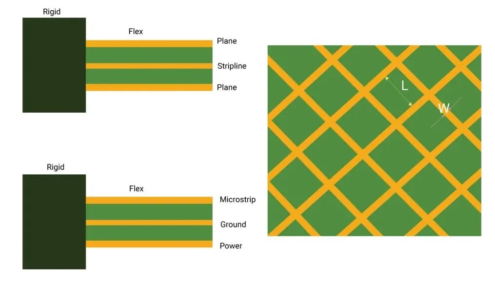
In a rigid PCB, a solid ground plane provides a consistent 0V reference and effective shielding across the entire board. In a flex area, a solid copper plane would make the circuit too stiff to bend. Designers must use alternative grounding structures — typically hatched or meshed ground planes — which provide shielding over a broad frequency range while still allowing the flex ribbon to bend without excessive rigidity.
However, hatched ground planes are less effective shields than solid copper. They have lower shielding isolation and modified conditions for impedance control. The mesh openings allow some electromagnetic energy to pass through, reducing shielding effectiveness.
2.2 The Signal Integrity Risk
Flexible circuits, by nature, are designed to route high-density signals across 3D geometries, often in devices where internal space is limited and reliability is mission-critical. These designs frequently support high-speed communication protocols like Ethernet, USB, CAN, or RF, where signal degradation or crosstalk due to EMI can result in data corruption, system errors, or outright failure.
When a flex area lacks proper shielding, emissions from high-speed traces can couple into adjacent signals, and external noise can couple into sensitive traces. The result is degraded signal integrity that may not appear until the device is in the field — under real operating conditions with real electromagnetic environments.
2.3 The Design Documentation Gap
Despite these risks, flex area shielding specifications are often missing from design files submitted for manufacturing. Common gaps include:
• Incomplete stack-up definitions: Shielding layers not specified in the flex area
• Missing hatch pattern details: No dimensions for mesh openings or trace widths
• Undefined grounding strategy: No via placement or ground connection specifications for shields
• Impedance requirements omitted: No controlled impedance specifications for traces over hatched planes
These gaps result in manufacturing delays, additional engineering queries, and — in some cases — boards that ship with inadequate shielding because the design did not specify what was needed.
3. Shielding Methods for Flex Areas
There are several shielding methods available for flex and rigid-flex circuits, each with distinct advantages, limitations, and design considerations.
3.1 Cross-Hatched Copper Layers
Cross-hatched copper layers are the most common shielding method for flex areas. A hatched or meshed ground plane is placed in the flex stack-up as a shielding layer. This provides a large conductor that can still provide shielding over a broad frequency range while allowing the flex ribbon to bend.
Advantages:
• Strong shielding effectiveness (second only to solid copper)
• Integrated into the stack-up during lamination — no post-processing required
• Compatible with controlled impedance designs
Limitations:
• Adds stiffness to the flex area
• Larger hatch openings reduce shielding effectiveness
• Requires careful impedance modeling — the mesh pattern affects characteristic impedance
Key design parameters:
• L (mesh opening): Increasing L opens the mesh, reduces shielding, and makes the ribbon easier to bend
• W (trace width): Increasing W closes the mesh, improves shielding, and makes the ribbon harder to bend
At high frequencies, the mesh pattern can start to resemble the glass weave pattern used in FR4, creating resonances that affect signal integrity. For L = 60 mils on polyimide, the first-order resonance occurs at approximately 50 GHz.
3.2 Shielding Films
Shielding films are pre-formed absorber materials with embedded metal particles and an adhesive backing. A film can be applied directly to the flex circuit surface. They are lightweight and effective in space-restricted designs.
Advantages:
• Lightweight and thin
• Can be applied to specific areas rather than the entire flex
• Effective shielding performance
• No impact on flex stack-up impedance
Limitations:
• Adds thickness and stiffness to the flex area
• Requires careful grounding — the shield must be electrically connected to ground
• Post-lamination application adds manufacturing steps
Shield films are ideal for applications where the flex area must remain as thin as possible and where adding copper layers is not feasible.
3.3 Silver Ink Shielding
Silver ink is screen-printed onto the flex circuit surface. It is more flexible and lightweight than copper but has lower conductivity.
Advantages:
• Highly flexible — conforms to bending
• Lightweight
• Can be applied to specific areas
Limitations:
• Lower conductivity than copper
• Most expensive shielding method
• Longest processing time
• Outdated for modern high-density or impedance-controlled designs
Silver ink is no longer recommended for modern rigid-flex applications with high-density or impedance-controlled requirements. It remains a legacy technology that has been largely superseded by shielding films and optimized copper hatch designs.
3.4 Comparison Summary
Table 1 — Flex area shielding methods comparison
| Method | Shielding Effectiveness | Flexibility | Cost | Best For |
|---|---|---|---|---|
| Cross-hatched copper | High | Moderate | Moderate | High-speed, controlled impedance designs |
| Shielding film | High | Moderate | Moderate-High | Space-restricted, lightweight designs |
| Silver ink | Moderate | High | Highest | Legacy designs; not recommended for new projects |
4. Design Details That Are Often Missing from Specifications
4.1 Inadequate Grounding Definition
A shield that is not properly grounded is ineffective — it becomes a floating conductor that can actually couple noise rather than blocking it.
What is often missing from design files:
• Insufficient grounding via placement connecting the shield layer to the main ground
• No specification for via spacing or pattern
• Missing ground return path definition at high frequencies
• No mention of shield connection to ground at the rigid-flex transition
Design guidance: Liberally specify grounding vias to connect shield layers and reference planes, preventing ground bounce. For high-frequency applications, use a "picket fence" pattern of vias to create a pseudo-Faraday cage around critical signal areas. Specify via spacing explicitly in your fabrication notes.
4.2 Shield Continuity Across the Rigid-Flex Transition
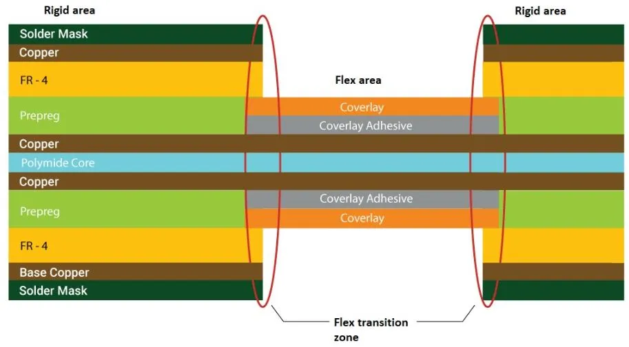
The transition from rigid to flex is where shielding often breaks down. Copper shielding layers that are solid in the rigid section must transition to hatched or removed in the flex section. The transition must be carefully designed to maintain shielding continuity.
What is often missing from design files:
• No definition of how the shield transitions from solid to hatched
• Missing alignment between rigid and flex shield layers
• Inconsistent hatch patterns specified across the transition
Design guidance: Specify the transition geometry in your fabrication drawing. Ensure that the hatch pattern in the flex area aligns with the solid plane in the rigid area to minimize discontinuities. Use a gradual transition rather than an abrupt change.
4.3 Shield Film Placement and Grounding Specifications
Shield films are applied after lamination, which requires clear specifications for placement and grounding.
What is often missing from design files:
• No dimensioned placement drawing for the shield film
• Missing grounding contact area specifications
• No requirement for adhesion verification
• Unclear whether the film should cover the entire flex or specific areas
Design guidance: Provide a detailed placement drawing for shield films. Specify the overlap area for grounding contact. Include adhesion testing requirements in your procurement specifications.
4.4 Impedance Requirements Over Hatched Planes
A hatched ground plane has higher characteristic impedance than a solid plane, which can shift impedance out of specification if not compensated.
What is often missing from design files:
• No impedance specification for traces over hatched planes
• No hatch pattern dimensions (L and W) provided
• Missing dielectric thickness requirements for the hatched section
Design guidance: Specify the target impedance for traces in the flex area. Provide the hatch pattern dimensions (mesh opening L and trace width W) so the manufacturer can verify impedance through simulation. Ensure the dielectric thickness is specified for accurate impedance control.
4.5 Odd-Layer Constructions for Two-Sided Shielding
Some designs require two-sided shielding in the flex areas, which is driven by stripline impedance control. This often requires odd-layer-count constructions.
What is often missing from design files:
• Assumption that even layer counts are required for all rigid-flex designs
• No consideration of the benefits of odd-layer flex constructions
• Missing specification for ground/signal/ground layer ordering
Design guidance: Recognize that odd-layer-count constructions are manufacturable and have distinct benefits. A ground/signal/ground construction contained within three layers of flex provides excellent two-sided shielding. Specify this stack-up explicitly in your design.
5. Design Guidelines for Effective Flex Area Shielding
5.1 When to Shield
Not every flex area needs shielding. Evaluate the need based on:
• Signal frequency: Higher frequencies require more shielding
• Signal sensitivity: Sensitive analog or RF signals need protection
• External environment: Will the device operate near other emitters?
• EMC requirements: What emissions and immunity standards must the product meet?
Shielding is typically used when a design is at risk of an emissions problem — something which can occur in flex designs without solid ground planes.
5.2 Shielding Method Selection
| Application Type | Recommended Method |
|---|---|
| High-speed digital (>1GHz), controlled impedance | Cross-hatched copper with impedance simulation |
| RF/microwave signals | Cross-hatched copper or shielding film |
| Space-constrained, lightweight designs | Shielding film |
| Legacy designs, cost-sensitive | Silver ink (not recommended for new designs) |
5.3 Stack-Up Design for Shielded Flex
For two-sided shielding (stripline configuration), use an odd-layer flex construction:
• Layer 1: Ground shield
• Layer 2: Signal layer
• Layer 3: Ground shield
This ground/signal/ground construction provides excellent shielding and is compliant with IPC-2223C. It also minimizes flex area thickness, providing improved flexibility and mechanical bend reliability.
5.4 Grounding Rules
• Place grounding vias every 5–10 mm along the shield perimeter
• Use multiple vias at shield connections to reduce inductance
• Ensure the shield has a low-impedance path to the main ground
• Avoid ground loops by using a single-point ground where possible
5.5 Hatch Pattern Optimization
• Balance shielding effectiveness with flexibility: larger openings = more flexibility, less shielding
• Simulate impedance over the hatch pattern — do not assume it matches solid plane impedance
• Use consistent hatch patterns across the flex area to avoid impedance discontinuities
• Consider using solid copper directly under critical traces and mesh elsewhere
5.6 What to Provide in Your Fabrication Package
To ensure your flex area shielding is manufactured correctly, include the following in your fabrication documentation:
• Stack-up diagram showing all shield layers in the flex area with thicknesses
• Hatch pattern dimensions (mesh opening L and trace width W) for each shield layer
• Impedance specifications for traces over hatched planes
• Ground via placement and spacing requirements for shield connections
• Shield film placement drawing (if applicable)
• Transition details from rigid to flex shield geometries
6. Summary: Shielding Is Not Optional
EMI shielding in the flex area of a rigid-flex PCB is not a luxury — it is a necessity for any design operating at high frequencies or in EMI-sensitive environments. Yet it is frequently missing from design specifications or inadequately defined.
The key takeaways:
• Flex areas are more vulnerable to EMI because grounding is harder to implement
• Cross-hatched copper is the most common and effective method, but it requires impedance simulation
• Shielding films offer a lightweight alternative for space-restricted designs
• Silver ink is outdated and not recommended for modern applications
• Grounding the shield must be specified explicitly with via placement details
• Odd-layer flex constructions enable two-sided shielding for stripline designs
• Provide complete shielding specifications in your fabrication package — do not assume defaults
A rigid-flex PCB with properly designed flex area shielding will pass EMC testing, maintain signal integrity, and perform reliably in the field. A design that omits or underspecifies flex area shielding may work in the lab but fail in the real world.
7. Frequently Asked Questions
Q1: Why is EMI shielding more challenging in flex areas than in rigid areas?
A: Flex areas cannot use solid copper ground planes because they would make the circuit too stiff to bend. Designers must use hatched or meshed ground planes, which have lower shielding effectiveness. Grounding is also harder to implement in flex regions.
Q2: What is the most effective shielding method for flex areas?
A: Cross-hatched copper layers integrated into the flex stack-up provide the strongest shielding after solid copper. They are compatible with controlled impedance designs and provide shielding over a broad frequency range.
Q3: Is silver ink shielding still recommended for rigid-flex PCBs?
A: No. Silver ink is outdated and not recommended for modern rigid-flex applications with high-density or impedance-controlled requirements. It is the most expensive shielding method and has the longest processing time.
Q4: How does a hatched ground plane affect impedance?
A: A hatched ground plane has higher characteristic impedance than a solid plane. The hatch pattern must be simulated and compensated for by adjusting trace widths or dielectric thickness. This should be specified in the design.
Q5: What shielding details should I include in my fabrication package?
A: Include: stack-up diagram with shield layers, hatch pattern dimensions (L and W), impedance specifications for traces over hatched planes, ground via placement details, and transition geometry from rigid to flex sections.
Q6: What is an odd-layer flex construction and why is it used for shielding?
A: An odd-layer flex construction has an odd number of flexible layers (e.g., 3 layers). It is used for designs that require two-sided shielding in the flex areas, driven by stripline impedance control. The ground/signal/ground construction provides excellent shielding.
Q7: How do hatch pattern parameters affect performance?
A: The mesh opening (L) and trace width (W) determine the fill factor. Increasing L opens the mesh, reducing shielding and making the ribbon easier to bend. Increasing W closes the mesh, improving shielding and making the ribbon harder to bend.
Q8: Can shielding films be used for dynamic bending applications?
A: Yes, but they add thickness and stiffness to the flex area. The film must be carefully placed and grounded. Adhesion should be verified to prevent delamination during bending.
Q9: When should I consider shielding for my flex area?
A: Consider shielding when the design is at risk of an emissions problem, which can occur in flex designs without solid ground planes. High-speed signals, sensitive analog or RF signals, and EMC compliance requirements all indicate a need for shielding.
Q10: Do all rigid-flex PCBs require flex area shielding?
A: No. Shielding is required only when the design includes high-speed signals, sensitive circuits, or must meet EMC compliance requirements. Low-speed, low-sensitivity designs may not need shielding.
8. About Richfulljoy
Richfulljoy specializes in high-reliability rigid-flex PCB manufacturing with comprehensive EMI shielding capabilities for the flex area. Our engineering team works closely with customers to ensure shielding is properly defined in the design, accurately manufactured, and verified through testing.
Our rigid-flex shielding capabilities:
• Cross-hatched copper: Custom hatch patterns with impedance simulation and verification
• Shielding films: Precision application with verified adhesion and grounding
• Odd-layer constructions: Ground/signal/ground flex stacks for two-sided shielding
• Stack-up design: Shield integration with bend radius and flexibility optimization
• Testing: Impedance verification, EMC pre-compliance testing
• Design support: Fabrication package review to identify missing shielding specifications
- Rigid-Flex PCB Lamination: Transition Slope Design for Rigid-Flex Thickness Differences
- Copper Grain Direction vs, Bending Axis; The First Principle Determining Dynamic Flex Life of Riaid-Flex PCBs
- Rigid-Flex PCB Bend Radius Limits: Dynamic vs Static Flex Life Differs by an Order of Magnitude
- Rigid-Flex Flex Area Routing: How Arc vs. 45° Corners Impact Dynamic Bend Life









