









RF PCB Spiral Inductor: Line Width Tolerance Accumulation Shifts Resonant Frequency by 5%
1. The Tolerance That Shifts Your Filter
A spiral inductor is one of the most fundamental passive components in RF and microwave PCB design. It appears in matching networks, resonant tanks, filters, VCOs, and impedance transformation circuits. Its geometry is simple — a planar spiral of copper trace on a dielectric substrate. Its electrical behavior, however, is exquisitely sensitive to the exact dimensions of that trace.
A typical RF PCB spiral inductor might have a design line width of 200μm. With standard PCB manufacturing tolerances, that line width can vary by ±10% or more — as wide as 180μm to 220μm. This variation changes the inductance, alters the self-resonant frequency, and shifts the entire circuit response.
The cumulative effect is not trivial. When line width tolerances accumulate across multiple turns of a spiral inductor, the resulting inductance variation can shift the resonant frequency by 5% or more — enough to detune a narrowband filter, shift a VCO frequency, or degrade matching network performance.
This article examines why line width tolerance has such a significant impact on spiral inductor performance, quantifies the relationship between line width variation and resonant frequency shift, and provides design strategies for achieving the RF performance your simulations promise.
2. The Planar Spiral Inductor: Geometry and Inductance
2.1 The Basic Structure
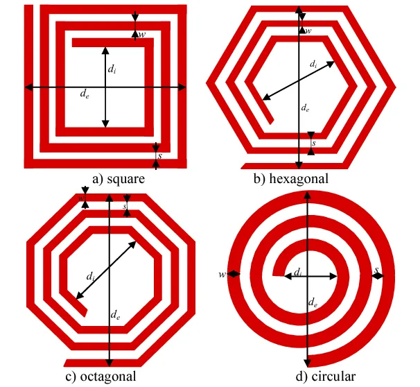
A planar spiral inductor on a PCB consists of a continuous copper trace wound in a spiral pattern — square, circular, octagonal, or rectangular. The conductor is typically 1/2 oz (17.5μm) to 1 oz (35μm) copper, with line width (W) and spacing (S) that are critical to performance.
The inductance of a planar spiral inductor depends on multiple geometric parameters:
• Line width (W): The width of the copper trace
• Line spacing (S): The gap between adjacent turns
• Number of turns (N): Total number of windings
• Outer diameter (D_out): The overall size of the spiral
• Inner diameter (D_in): The diameter of the central opening
• Trace thickness (t): The copper foil thickness
Among these parameters, line width is the most variable in manufacturing and has a direct, first-order effect on inductance.
2.2 How Line Width Affects Inductance
The inductance of a planar spiral inductor is not a simple function of line width alone — it depends on the complex interaction of magnetic fields between adjacent turns. However, the relationship is well understood:
Narrower traces increase inductance per unit length. When trace width decreases, the current density increases, and the magnetic field becomes more concentrated. For a rectangular trace over a ground plane, decreasing the width increases the inductance per unit length and decreases the capacitance per unit length, thus increasing the characteristic impedance.
Wider traces decrease inductance but improve Q-factor. Wider traces have lower DC resistance, which reduces ohmic losses and improves the quality factor (Q). However, wider traces also increase parasitic capacitance to the ground plane, which lowers the self-resonant frequency.
The practical consequence is a trade-off: a 10% reduction in line width can increase inductance by several percent, while a 10% increase in line width can decrease inductance by a similar amount. In a spiral inductor with multiple turns, this variation accumulates across every turn.
Table 1 — Sensitivity of spiral inductor parameters to line width variation
| Parameter | Effect of Line Width Reduction | Effect of Line Width Increase |
|---|---|---|
| Inductance (L) | Increases | Decreases |
| DC resistance (Rdc) | Increases | Decreases |
| Q-factor | Decreases (higher loss) | Increases (lower loss) |
| Parasitic capacitance (Cp) | Decreases | Increases |
| Self-resonant frequency (f_sr) | Increases | Decreases |
3. The Tolerance Chain: From Design to Finished Board
3.1 Where Line Width Variation Comes From
The line width of a PCB trace is not perfectly controlled. Multiple manufacturing steps introduce variation:
Photolithography: The artwork (film or direct imaging) defines the trace pattern. Film shrinkage can introduce ±1.5 mil (38μm) error. Laser Direct Imaging (LDI) improves this to ±0.6 mil (15μm).
Etching: The wet etching process removes unwanted copper. The etchant attacks not only vertically but also laterally — undercutting the photoresist. This side-etch reduces the final trace width. Standard subtractive etching produces ±20% line width variation due to undercut and sidewall angle.
Copper thickness variation: Copper foil thickness varies by ±10% for standard half-ounce copper. Thicker copper requires longer etching time, increasing side-etch and further reducing trace width.
Panel position: Etch rate varies across the panel — traces at the panel center may etch differently from traces at the edges. The etch compensation applied during artwork generation must account for copper thickness and panel position.
3.2 The Accumulation Effect
The critical insight is that line width tolerance does not affect just one turn of a spiral inductor. It affects every turn — and the effects accumulate.
Consider a 6-turn spiral inductor with a design line width of 200μm. If the manufacturing tolerance is ±10% (±20μm), each turn may be 180μm or 220μm. The inductance contribution of each turn depends on its actual width. The total inductance is the sum of the contributions from all turns.
If all turns are consistently narrow (180μm) or consistently wide (220μm), the total inductance shift is the sum of per-turn shifts. If the variation is random (some turns narrow, some wide), the net effect is more complex but still significant.
The result: a ±10% line width tolerance can produce a ±5-8% inductance variation in a multi-turn spiral inductor.
3.3 The Resonant Frequency Connection
The self-resonant frequency (f_sr) of a spiral inductor is determined by the inductance (L) and the parasitic capacitance (C_p):
f_sr = 1 / (2π √(L × C_p))
When line width varies, both L and C_p change — and they change in opposite directions:
• Narrower traces: L increases, C_p decreases → f_sr increases significantly
• Wider traces: L decreases, C_p increases → f_sr decreases significantly
This is the mechanism behind the 5% resonant frequency shift. The combined effect of inductance and capacitance variation from line width tolerance can shift the self-resonant frequency by 5% or more.
Table 2 — Resonant frequency shift from line width variation
| Line Width Change | Inductance Change | Capacitance Change | Resonant Frequency Shift |
|---|---|---|---|
| -10% (narrower) | +3-5% | -3-5% | +4-7% (increases) |
| +10% (wider) | -3-5% | +3-5% | -4-7% (decreases) |
| ±10% (worst case) | ±5% | ±5% | ±5-7% |
A 5% shift in resonant frequency is enough to move a 2.4 GHz filter off its center frequency by 120 MHz — well beyond acceptable limits for most RF systems.
4. Quantifying the Impact: Research and Data
4.1 Line Width vs. Impedance: The 10% / 6% Relationship
Research on differential interconnects has quantified the relationship between line width variation and impedance change. A 10% change in trace width produces a change of approximately 6% in differential impedance for 17.5μm trace thickness. For 35μm trace thickness, the change is about 5.6%.
This relationship scales to inductance: a 10% line width variation produces approximately a 5-6% inductance variation.
4.2 The Self-Resonant Frequency Impact
Studies on spiral resonators in PCB environments have demonstrated that the self-resonant frequency can vary within an 8% tolerance between measurement and simulation, with line width and spacing variations being primary contributors.
In practical terms, a PCB etching tolerance variation of ±10% in line width can result in a filter center frequency variation of 3%. For multi-turn spiral inductors with cumulative effects, this can reach 5% or more.
4.3 The Etching Tolerance Challenge
Research on PCB etching tolerances has shown that variations in line width directly affect both inductance and capacitance. One approach to compensate is to design the circuit such that the decrease in capacitance from etching is balanced against the increase in inductance from the same etching — effectively canceling the resonant frequency shift.
However, this compensation is design-specific and requires precise control of the etching process. Without compensation, the resonant frequency variation remains a significant challenge.
5. Design Strategies for Controlling Resonant Frequency Shift
5.1 Specify Tighter Line Width Tolerances
The most direct approach is to specify tighter manufacturing tolerances.
| Application | Standard Tolerance | Recommended RF Tolerance |
|---|---|---|
| General purpose | ±20% | ±10% |
| RF (<6 GHz) | ±15% | ±10% |
| RF (6-40 GHz) | ±10% | ±5% |
| Millimeter-wave (>40 GHz) | ±10% | ±3% or better |
IPC-6012 Class 3 specifies conductor width tolerances of ±10%. For millimeter-wave applications, even tighter control is required.
Specify the requirement on your fabrication drawing. Include line width tolerance as a critical-to-quality parameter for any spiral inductor.
5.2 Use Laser Direct Imaging (LDI)
Traditional film-based photolithography introduces film shrinkage and alignment errors that compound line width variation. LDI eliminates film-related errors, improving line width control from ±20% to ±10% or better.
For RF PCBs with spiral inductors, LDI is not optional — it is a requirement for achieving consistent inductance values.
5.3 Design for Manufacturing Tolerances
Account for line width variation during the design phase:
Simulate with tolerance bounds. Run electromagnetic simulations with line width varied by ±10%. If the resonant frequency shift exceeds your specification, tighten the tolerance or redesign.
Use wider traces where possible. Wider traces are less sensitive to percentage variation. A ±10% variation on a 300μm trace is ±30μm; on a 100μm trace, it is ±10μm — but the percentage impact on inductance is similar.
Consider tapered inductors. Variable line width designs — where the line width increases toward the outer turn — can improve Q-factor and may offer better tolerance control.
5.4 Include Test Coupons
Include inductance test coupons on the production panel — separate spiral inductors with the same geometry as the design. Measure the inductance of these coupons after fabrication to verify that the line width tolerance achieved the target inductance.
For critical RF designs, specify 100% inductance testing on the production lot.
5.5 Consider Post-Fabrication Tuning
For very tight frequency requirements, consider post-fabrication tuning:
• Laser trimming: Remove small amounts of copper to adjust inductance
• Component selection: Use tunable capacitors or trimmer capacitors in parallel with the inductor
• Selective assembly: Measure each inductor and select matching components
6. Summary: The 5% Reality
The line width tolerance of a PCB spiral inductor is not a minor manufacturing detail. It is a first-order performance parameter that directly determines the resonant frequency of RF circuits.
The key takeaways:
• Line width tolerance accumulates across multiple turns of a spiral inductor
• A ±10% line width variation produces approximately ±5-6% inductance variation
• Resonant frequency shifts by 5% or more due to combined L and C variation
• Standard PCB tolerances (±20%) are inadequate for RF spiral inductors
• Specify ±10% or tighter for RF applications above 1 GHz
• Laser Direct Imaging (LDI) is required for consistent line width control
• Simulate with tolerance bounds and verify with test coupons
A PCB spiral inductor designed with tight line width control — ±10% or better — will achieve the resonant frequency your simulations predict. A design that accepts standard manufacturing tolerances may measure 5% off frequency — the difference between a working RF circuit and one that fails specification.
7. Frequently Asked Questions:
Q1: Why does line width tolerance affect spiral inductor resonant frequency?
A: Line width variation changes both the inductance (L) and the parasitic capacitance (C_p) of the inductor. Narrower traces increase L and decrease C_p, raising the resonant frequency. Wider traces decrease L and increase C_p, lowering the resonant frequency.
Q2: What line width tolerance is typical for standard PCB manufacturing?
A: Standard subtractive etching produces ±20% line width variation. IPC-6012 Class 2 and Class 3 specify ±10% conductor width tolerances.
Q3: How much does a 10% line width change affect inductance?
A: Research shows that a 10% change in trace width produces approximately a 6% change in differential impedance. For spiral inductors, this translates to a 5-6% inductance variation.
Q4: What is the resonant frequency shift from ±10% line width tolerance?
A: The combined effect of inductance and capacitance variation can shift the self-resonant frequency by 5% or more. For a 2.4 GHz filter, this is a 120 MHz shift.
Q5: How can I specify line width tolerance on my fabrication drawing?
A: Include a note: "Conductor width tolerance for all RF traces and spiral inductors: ±10% maximum per IPC-6012 Class 3. Laser Direct Imaging (LDI) required. Inductance test coupons to be included on panel."
Q6: Does line spacing tolerance also affect inductor performance?
A: Yes, but less significantly. The 50% change in the trace space showed a change of less than 1% in differential impedance. Line width has a much stronger effect than line spacing.
Q7: What is the best way to verify inductor performance after fabrication?
A: Include inductance test coupons on the production panel — separate spiral inductors with identical geometry. Measure inductance using an impedance analyzer or VNA. Compare measured values against simulation to verify line width control.
Q8: Can I compensate for line width variation in my circuit design?
A: Yes. Use tunable components (trimmer capacitors) in parallel with the inductor. Design the circuit to be tolerant of ±5-10% inductance variation. Use wider traces where possible to reduce percentage variation.
Q9: What manufacturing technology improves line width control?
A: Laser Direct Imaging (LDI) eliminates film shrinkage errors. Controlled-depth etching reduces variation to ±10%. Modified semi-additive processes achieve ±10μm absolute tolerance.
Q10: Does copper thickness affect line width tolerance?
A: Yes. Thicker copper requires longer etching time, increasing side-etch and line width variation. Thinner copper (1/2 oz / 17.5μm) provides better line width control than 1 oz (35μm) copper.
8. About Richfulljoy
Richfulljoy specializes in high-precision RF and microwave PCB manufacturing with tight line width control for spiral inductors, filters, and impedance-controlled structures.









