Blog
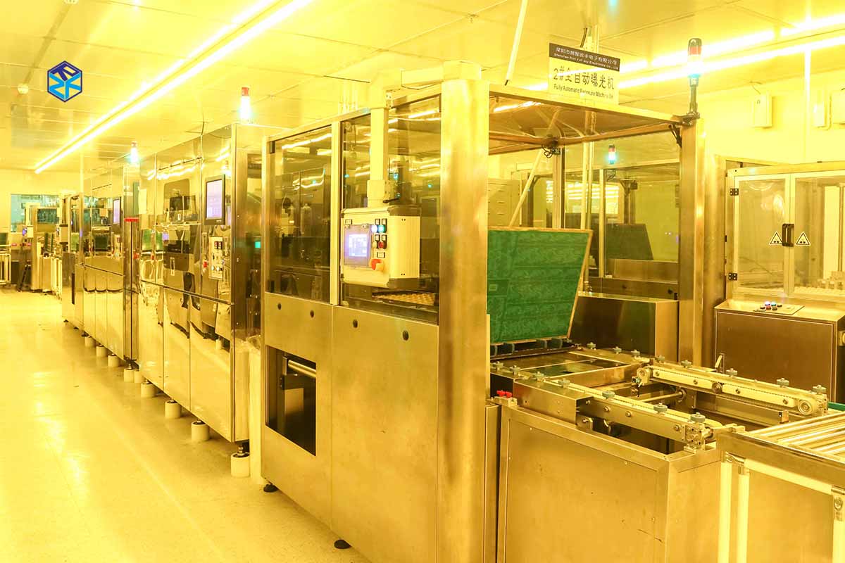
Circuit Exposure Ink Exposure LDI exposure speed
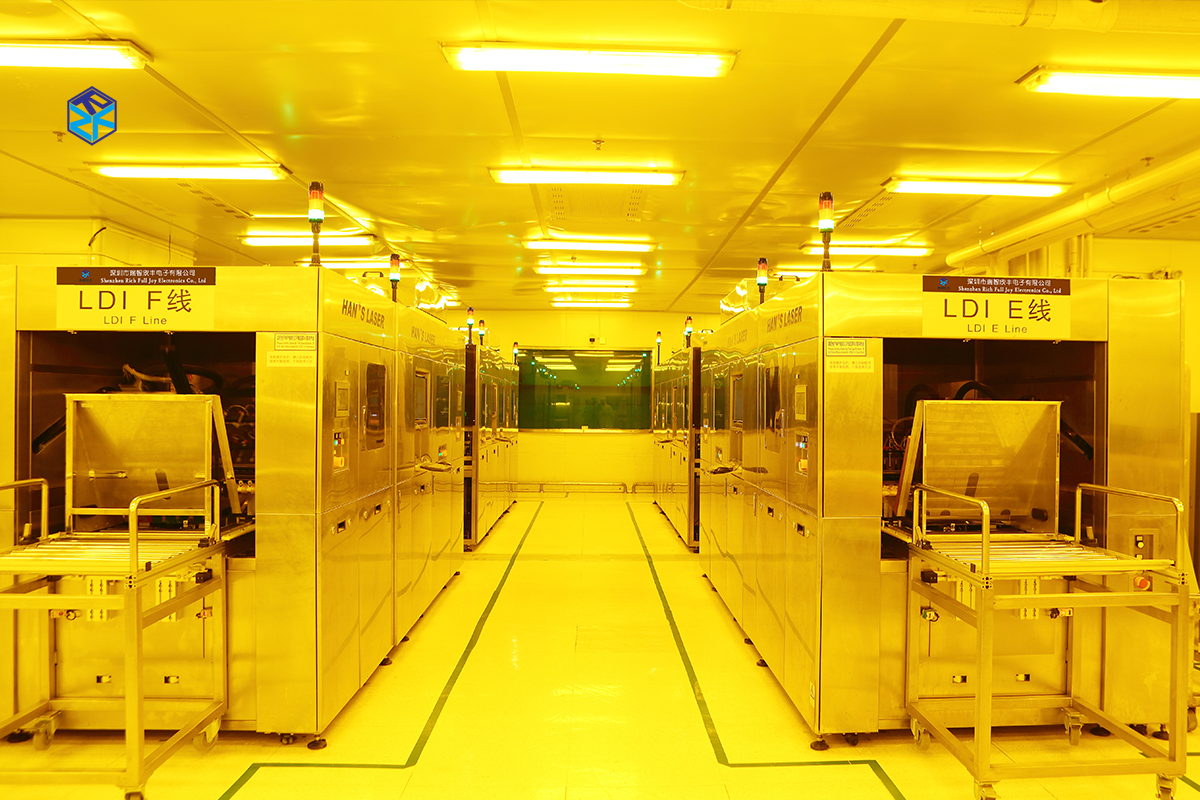
In the production process of Printed Circuit Boards (PCBs), exposure is a crucial step. Many PCB manufacturers use CCD semi-automatic exposure machines for this process, but Shenzhen Rich Full Joy Electronics Co., Ltd. has introduced LDI direct imaging exposure machines, a technology that offers numerous advantages. However, LDI exposure speed is relatively slow.
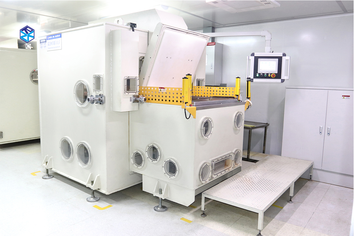
Plugging Process - Vacuum Resin Plugging Machine-B
echnical Highlights, Production Process, Precautions, and Defect Prevention
The vacuum resin plugging process is essential in modern PCB manufacturing, particularly for multilayer boards, high-density interconnects (HDI), and rigid-flex boards. The Vacuum Resin Plugging Machine-B uses vacuum technology to evenly fill holes with resin, enhancing the electrical performance, mechanical strength, and reliability of products. Below is a detailed introduction to the technical highlights, production process, key precautions, and methods for preventing defects in this process.
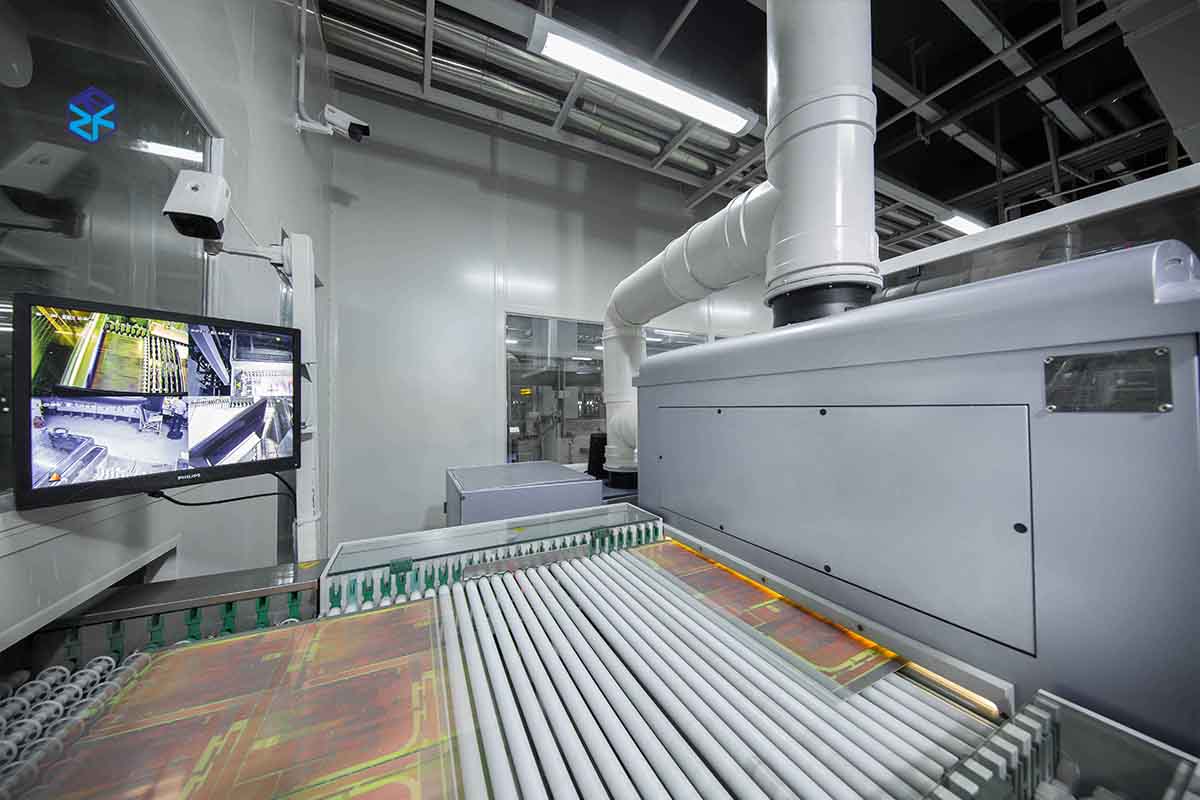
PCB Inspection - Online AOI
In the production of PCBs (Printed Circuit Boards), precise defect inspection is crucial for ensuring product quality. Below are descriptions of common PCB defects
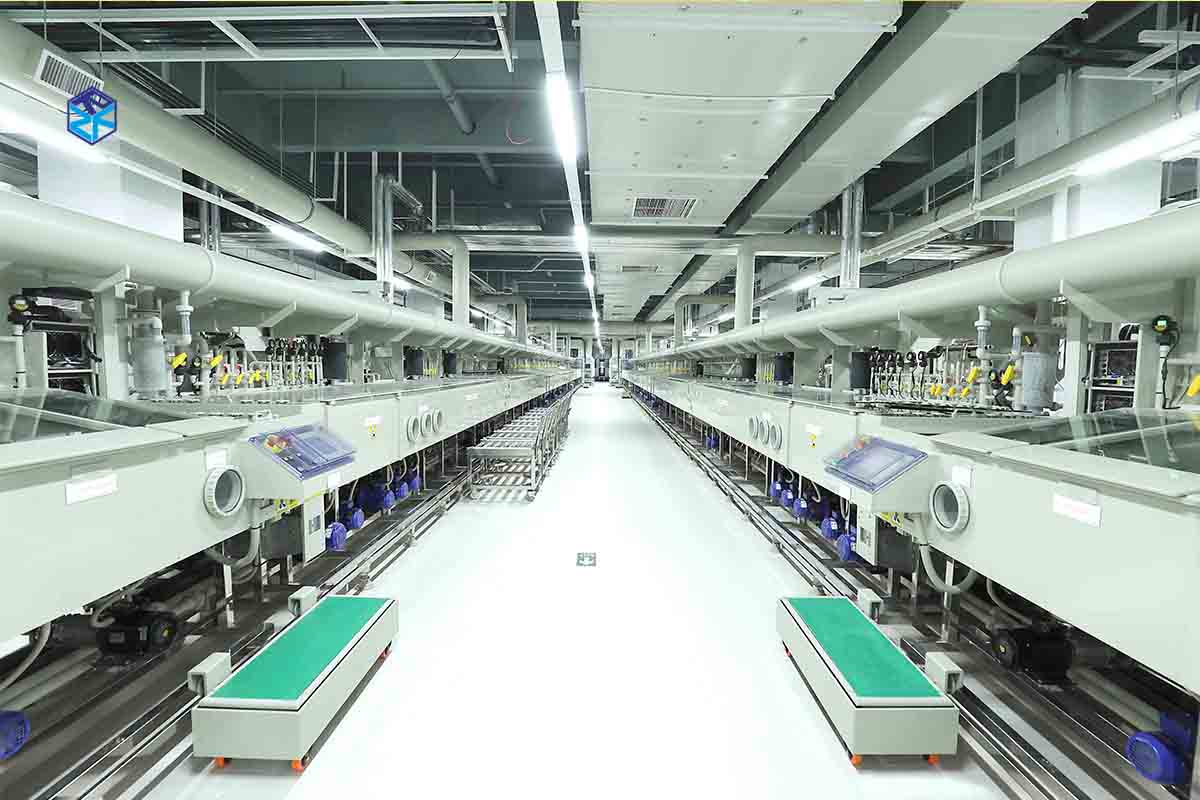
PCB Hole Copper Plating - Via Filling Plating Lines
The Role of Via Filling Plating Lines
Via filling plating lines are crucial in the PCB manufacturing process, ensuring the functionality and reliability of electronic devices.
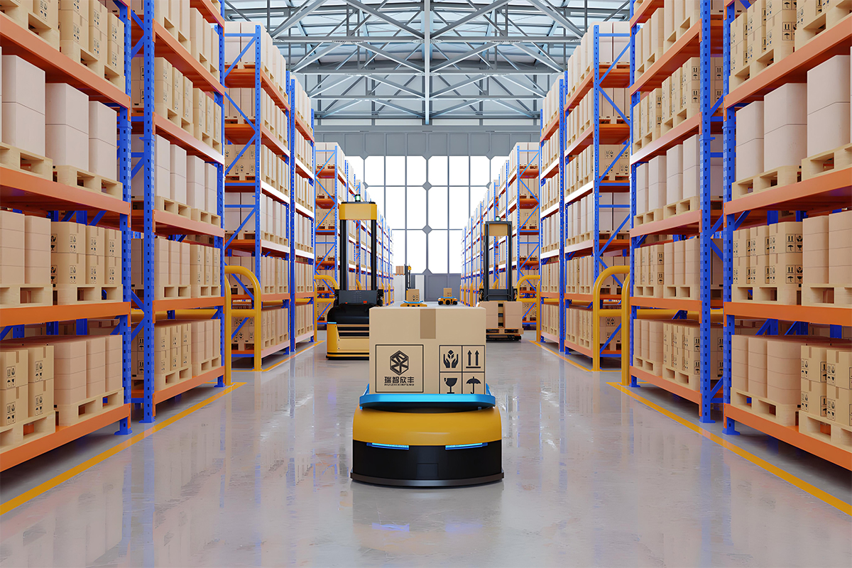
Shenzhen Rich Full Joy Electronics Co., Ltd Introduces Intelligent Warehousing and Handling Robots: Enhancing PCB Production Efficiency and Management Precision
In the PCB (Printed Circuit Board) manufacturing process, efficient material management is crucial for ensuring production efficiency, reducing costs, and maintaining product quality.
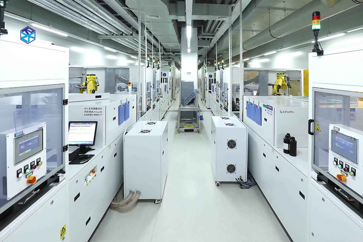
What Are the Key Operating Principles and Technical Parameters for Post-Inkjet Curing on PCBs to Reduce Defects?
Ensure the inkjet head and oven are clean and free from contaminants. Check all components are functioning properly.
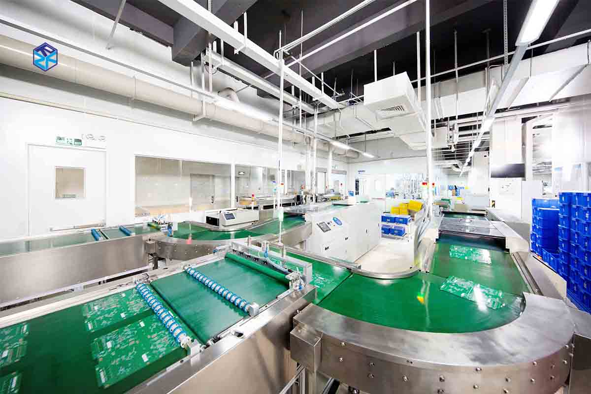
Finished PCB Cleaning Line Features: Board Bending and Warping Detection
Comprehensive Detection Functions: The finished PCB cleaning line not only cleans PCBs but also features board bending and warping detection to ensure the flatness and quality of the finished product.
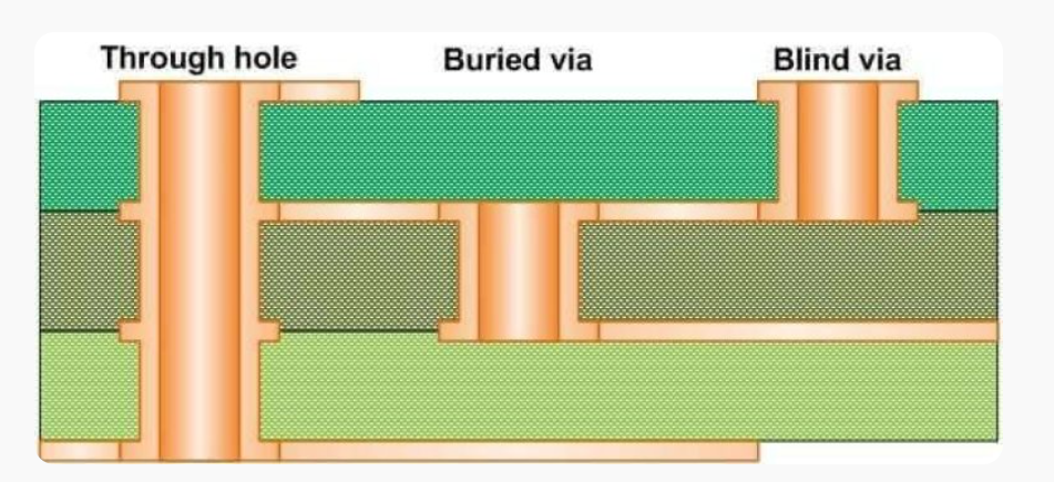
What is via in PCB?
Vias are the most common holes in PCB production. They connect the different layers of the same network but are usually not used for solder components. Vias can be divided into three types: through holes, blind vias, and buried vias. The details information for these three vias is as below:
What is a printed circuit board?
PCB Trace Manufacturing Process: Equipment, Techniques, and Key Considerations
The manufacturing of Printed Circuit Board (PCB) traces is a critical step in the PCB production process. This process involves multiple stages, from circuit design to the actual formation of traces, ensuring that the final product performs reliably. Below is a detailed summary of the equipment, processes, and key considerations involved in trace manufacturing.