











Optical Module Microstrip-to-CPW Transition: Etching Compensation Accuracy Determines Bandwidth
1. Introduction
The relentless march toward 400G, 800G, and emerging 1.6T optical transceivers has pushed PCB signal integrity requirements to their physical limits. Within the confined footprint of an optical module — typically a QSFP-DD or OSFP form factor — multiple transmission line types must coexist: microstrip lines for high-speed digital routing, grounded coplanar waveguide (GCPW) for RF driver outputs, and delicate transitions that connect them.
Among all the discontinuities in an optical module PCB, the microstrip-to-coplanar waveguide transition is perhaps the most critical and the most unforgiving. It is here that the electromagnetic field must rearrange itself from the microstrip's asymmetric distribution — field concentrated between the signal trace and the distant ground plane below — to the GCPW's tightly confined field between the signal line and the adjacent ground traces on the same layer.
If this transition is poorly executed, the bandwidth of the entire RF path collapses. Reflections accumulate, insertion loss spikes, and the eye diagram closes. The 100G per lane or 200G per lane signals that define modern optical modules simply cannot pass.
What determines whether a transition succeeds or fails? The answer, increasingly clear from both simulation and production data, is etching compensation accuracy. Not the dielectric material. Not the stack-up design alone. The precision with which the PCB manufacturer compensates for the inevitable lateral etching of copper traces during the wet etch process.
2. Why Microstrip and CPW Do Not Naturally Match
2.1 The Field Distribution Problem
A microstrip line consists of a signal trace on the top layer with a solid ground plane on the layer beneath. The electromagnetic field is distributed between the trace and the ground plane, with significant fringing fields extending into the air above the board. The characteristic impedance is primarily determined by the trace width, the dielectric thickness, and the material's dielectric constant.
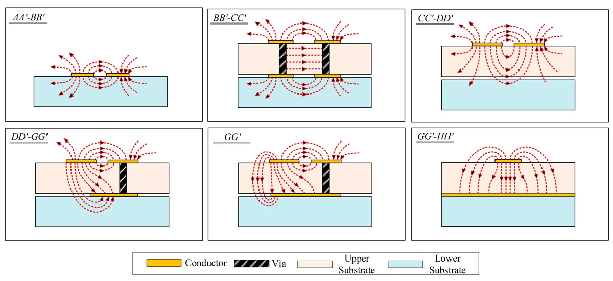
A grounded coplanar waveguide, by contrast, places ground traces on the same layer as the signal line, separated by narrow gaps, with an additional ground plane underneath. The field is much more tightly confined to the surface region, with the gaps between signal and ground carrying a substantial portion of the electromagnetic energy.
When a microstrip line transitions to a GCPW, the field must reconfigure. The ground reference shifts from a distant plane below to adjacent coplanar conductors. The impedance changes. The propagation constant changes. Without careful design, this transition creates a strong reflection — a bandwidth-limiting discontinuity.
2.2 The Impedance Matching Illusion
Many designers assume that if they set the microstrip and the GCPW to the same nominal impedance — typically 50Ω — the transition will be seamless. This is incorrect. Even with identical characteristic impedance, the field distributions are fundamentally different. The transition region must gradually transform not only the impedance but also the field configuration.
This transformation is typically achieved through a tapered or stair-shaped transition structure, where the GCPW signal line width and gap dimensions are progressively adjusted. The geometry of this transition — every line width, every gap dimension, every taper length — must be manufactured with extreme precision. And this is where etching compensation enters the picture.
3. The Etching Process and Its Inevitable Errors
3.1 How Wet Etching Works
PCB fabrication relies on wet etching to remove unwanted copper from the board. A photoresist pattern defines the desired copper traces, and the board is immersed in an etchant solution (typically alkaline or acidic) that dissolves the exposed copper. The photoresist protects the intended copper features.
However, etching is not perfectly vertical. The etchant attacks copper not only downward but also laterally — undercutting the photoresist. This lateral etching, known as side-etch or undercut, means that the final copper trace is narrower than the photoresist pattern that defined it. The cross-section of a traced becomes trapezoidal rather than rectangular.
For a standard microstrip line with widths measured in millimeters, a few micrometers of side-etch are negligible. For the dimensions encountered in optical module transitions — where GCPW signal lines may be only 80μm wide and gaps only 40μm wide — a few micrometers of side-etch represent a percentage error of several percent.
3.2 The Dimensional Error Chain
The manufacturing tolerances that affect a microstrip-to-CPW transition include:
| Parameter | Typical Tolerance | Impact on 50Ω GCPW |
|---|---|---|
| Etched line width (W) | ±2 μm | ±2.8 Ω impedance shift |
| Gap dimension (G) | ±3 μm | ±6.2 Ω impedance shift |
| Dielectric thickness | ±8% | ~4.1 Ω shift per 5% change |
| Copper thickness | ±12% | Affects loss, less impact on Z0 |
| Layer-to-layer registration | <±15 μm | Phase error in coupled structures |
The gap dimension is the most sensitive. A ±3μm variation in the gap — entirely typical for standard PCB etching — produces a 12.4% impedance variation. For a transition designed to match 50Ω to 50Ω, this variation alone can push the impedance to 56Ω or down to 44Ω, creating a reflection coefficient that severely limits bandwidth.
Even more concerning is the phase impact. At 60 GHz, a 2μm increase in the gap causes an 11.3° phase lag over a 10cm GCPW line. In an optical module with tightly controlled timing requirements, this phase error translates directly to degraded signal integrity.
4. Etching Compensation: The Bridge Between Design and Reality
4.1 What Is Etching Compensation?
Etching compensation is the deliberate pre-distortion of the artwork data to counteract the inevitable side-etch. If the PCB manufacturer knows that a 100μm design-width trace will etch to only 95μm, they widen the photoresist pattern to 105μm so that the final etched trace measures the intended 100μm.
The compensation is quantified by the etch compensation coefficient (Ketch):
Ketch = (Wdesign − Wmeasured) / Wdesign
Where Wdesign is the designed (CAD) line width and Wmeasured is the actual etched width.
4.2 Why Ketch Is Not a Constant
A critical insight: Ketch is not a fixed number that applies uniformly across the board. It depends on multiple variables:
• Copper thickness: Thicker copper requires longer etching time, which increases lateral undercut. For 12μm (½ oz) copper, Ketch typically ranges from 0.8 to 1.2 mils. For 28μm (1 oz) copper, Ketch can reach 1.5 to 2.2 mils.
• Line width: Narrower lines are proportionally more affected by side-etch than wider lines. When line width falls below 4 mils (approximately 100μm) and copper thickness exceeds 28μm, Ketch shows a strong negative correlation with line width.
• Etchant chemistry: Temperature, concentration, and agitation all affect the etch rate and the lateral-to-vertical etch ratio.
• Photoresist resolution: Finer photoresist features are more susceptible to edge roughness and development variations.
For an optical module transition, where line widths may vary from 80μm (GCPW signal) to 200μm (microstrip) within the same transition structure, a single compensation value cannot work. The narrow GCPW features require different compensation than the wider microstrip features.
4.3 The Transition-Specific Compensation Challenge
The microstrip-to-CPW transition is uniquely sensitive to compensation errors because it contains multiple geometries that must match precisely:
• The microstrip line width (relatively wide, less sensitive)
• The GCPW signal line width (narrow, highly sensitive)
• The GCPW gap width (extremely sensitive — the most critical dimension)
• The taper or stair-step dimensions that bridge them
If the compensation is inaccurate for the gap dimension, the transition's impedance profile deviates from the design. If the compensation differs between the signal line and the gap (which it often does, because they have different geometries), the impedance matching across the transition is destroyed.
The result: The transition bandwidth collapses. What was designed as a DC-to-40GHz transition may measure only DC-to-25GHz in production.
5. How Etching Compensation Accuracy Determines Bandwidth
5.1 The Bandwidth-Defining Mechanism
The bandwidth of a microstrip-to-CPW transition is determined by four dominant factors:
1. Energy leakage in the GCPW section
2. Field match along the transition
3. Impedance match along the transition
4. Physical dimensions and their manufacturing accuracy
Factors 2 and 3 are design choices — they can be optimized through electromagnetic simulation. Factor 1 is material-dependent. But factor 4 is where manufacturing precision, and specifically etching compensation, determines the outcome.
When etching compensation is inaccurate:
• The impedance profile along the transition no longer matches the design
• Reflections occur at multiple points along the transition, not just at the endpoints
• These reflections combine constructively at certain frequencies, creating notches in the S11 response
• The usable bandwidth — defined as the frequency range where return loss remains below -10dB — shrinks
A well-compensated transition with ±1μm dimensional accuracy can achieve bandwidths exceeding 40GHz or even 100GHz with optimized via structures. A poorly compensated transition with ±3μm errors may struggle to reach 25GHz — insufficient for 400G optical modules operating at 53 Gbaud (Nyquist frequency ~26.5GHz) or 800G modules at 106 Gbaud (~53GHz).
5.2 Quantifying the Impact
Consider a 50Ω GCPW-to-microstrip transition designed for a 400G optical module (operating at 53 Gbaud PAM4, with significant energy up to ~30GHz). The design calls for:
• GCPW signal width: 80μm
• GCPW gap: 40μm
• Microstrip width: 180μm
• Transition taper length: 500μm
With perfect etching compensation, the transition achieves S11 < -15dB from DC to 35GHz.
Now consider two manufacturing scenarios:
Scenario A — Standard compensation (±3μm accuracy on gaps) :
The gap measures 43μm instead of 40μm. Impedance shifts from 50Ω to approximately 56Ω. Return loss at 28GHz degrades to -10dB — marginal. The module passes initial test but fails at temperature extremes.
Scenario B — Precision compensation (±1μm accuracy on gaps, achieved through careful Ketch characterization and per-feature compensation) :
The gap measures 40.5μm. Impedance remains within 51Ω. Return loss stays below -15dB across the band. The module meets specification with margin.
The difference between these scenarios is not the design. It is not the material. It is the accuracy of etching compensation.
6. Achieving Etching Compensation Accuracy for Optical Module PCBs
6.1 Characterizing the Process
The first step toward accurate compensation is characterization. The PCB manufacturer must run test coupons — panels with multiple line widths and gap dimensions — through the exact production process. TDR measurements reveal the actual impedance achieved for each geometry. From these measurements, the effective etched dimensions can be back-calculated, and Ketch values can be derived for each geometry class.
For optical module transitions, this characterization must be geometry-specific. A single Ketch value for the entire board is insufficient. The narrow GCPW features require different compensation than the wider microstrip features. The gaps — the most critical dimension — require the most careful characterization.
6.2 Per-Feature Compensation
With characterized Ketch values, the CAM (Computer-Aided Manufacturing) team can apply per-feature compensation:
• Microstrip lines: widen by Ketch_ms
• GCPW signal lines: widen by Ketch_gcpw_signal
• GCPW gaps: adjust the ground trace positions by Ketch_gap
This is not a simple global scaling. It is a targeted adjustment of each geometry based on its specific etch behavior.
For transitions with line widths below 4 mils (100μm) and copper thickness above 28μm, the compensation may need to be nonlinear — the relationship between design width and etched width is not linear in this regime. Linear compensation will produce systematic errors.
6.3 Verification Through Coupon Testing
Every production panel for optical module PCBs should include impedance coupons that replicate the critical transition geometries. TDR testing of these coupons provides real-time feedback on whether the compensation is achieving the target impedance.
For GCPW structures, specialized calibration is required. Traditional SMA-to-microstrip probes introduce discontinuities that mask the true GCPW impedance. Custom GCPW-to-GCPW TRL calibration kits, with precision delay lines and matched loads, provide the accuracy needed for millimeter-wave verification.
7. Summary: Precision Is Not Optional
The microstrip-to-coplanar waveguide transition is the bandwidth bottleneck in optical module PCB design. Its performance depends not only on the electromagnetic design but critically on the manufacturing accuracy of the transition geometry.
Etching compensation — the deliberate pre-distortion of artwork to counteract side-etch — is the primary tool for achieving this accuracy. But compensation must be:
• Characterized through process-specific test coupons
• Per-feature, not global — narrow GCPW lines and gaps behave differently from wider microstrip lines
• Verified through TDR testing of production coupons
When etching compensation is inaccurate, the transition bandwidth collapses. When it is precise — when the gap dimension is held to ±1μm rather than ±3μm — the transition delivers the bandwidth that the optical module requires.
For 400G, 800G, and beyond, etching compensation accuracy is not a manufacturing detail. It is a bandwidth-defining parameter.
8. Frequently Asked Questions (FAQ)
Q1: Why is the microstrip-to-CPW transition particularly sensitive to etching errors?
A: Because the transition contains multiple geometries (microstrip line, GCPW signal, GCPW gaps) that must match precisely. The gaps are the most critical — a ±3μm variation changes impedance by over 12%, destroying the impedance match across the transition.
Q2: What is etching compensation and why is it needed?
A: Etching compensation is the deliberate widening of photoresist patterns to counteract the lateral undercut (side-etch) that occurs during wet etching. Without compensation, the final etched trace is narrower than designed, shifting impedance and degrading bandwidth.
Q3: Can a single compensation value work for the entire optical module PCB?
A: No. Different geometries etch differently. Narrow GCPW lines require different compensation than wider microstrip lines. The gaps — the most critical dimension — require their own compensation. Per-feature compensation is essential.
Q4: How much does a 2μm gap error affect GCPW performance at millimeter-wave frequencies?
A: A 2μm increase in the gap shifts impedance by approximately 4Ω and causes an 11.3° phase lag at 60 GHz over a 10cm line. This phase error degrades beamforming and signal timing in high-speed optical modules.
Q5: What is the typical impedance tolerance achievable with standard PCB etching?
A: Standard ±10% trace width control yields approximately ±5% impedance tolerance. For precision RF applications, ±3% is achievable with tighter process control and material selection. Optical module transitions typically require the tighter tolerance.
Q6: How does copper thickness affect etching compensation?
A: Thicker copper requires longer etching time, increasing lateral undercut. For 28μm (1 oz) copper, Ketch can reach 1.5–2.2 mils, compared to 0.8–1.2 mils for 12μm (½ oz) copper. Compensation values must be adjusted for copper thickness.
Q7: What is the relationship between line width and compensation accuracy?
A: When line width falls below 4 mils (approximately 100μm), the relationship between design width and etched width becomes nonlinear. Simple linear compensation produces systematic errors. Nonlinear compensation or per-geometry characterization is required.
Q8: How is etching compensation verified in production?
A: Through impedance coupons that replicate the transition geometries. TDR testing of these coupons reveals whether the compensation achieved the target impedance. For GCPW, specialized TRL calibration is required for accurate measurement.
Q9: What bandwidth can a well-compensated microstrip-to-CPW transition achieve?
A: With precise compensation (±1μm dimensional accuracy), transitions can achieve bandwidths exceeding 40GHz and up to 100GHz with optimized via structures. Poor compensation may limit bandwidth to 25GHz or less.
Q10: Why is gap dimension control more critical than signal line width control?
A: The GCPW gap dimension has a much stronger effect on impedance than the signal line width. A ±3μm gap variation causes ±6.2Ω impedance shift, compared to ±2.8Ω for a ±2μm line width variation. Gap control is the priority for transition bandwidth.
9. About Richfulljoy
Richfulljoy specializes in high-precision PCB manufacturing for optical modules, RF front-ends, and millimeter-wave applications. Our manufacturing capabilities include:
• Precision etching: Per-feature compensation with characterized Ketch values for geometries down to 2 mils (50μm)
• Impedance control: ±5% standard, ±3% for precision RF applications
• Material capabilities: Rogers RO4000 series, Megtron 6, Isola Astra, PTFE, and hybrid stack-ups
• Testing: TDR impedance verification with GCPW-specific TRL calibration
• Documentation: Full impedance test reports, cross-section analysis, and first-article inspection









