











Blog
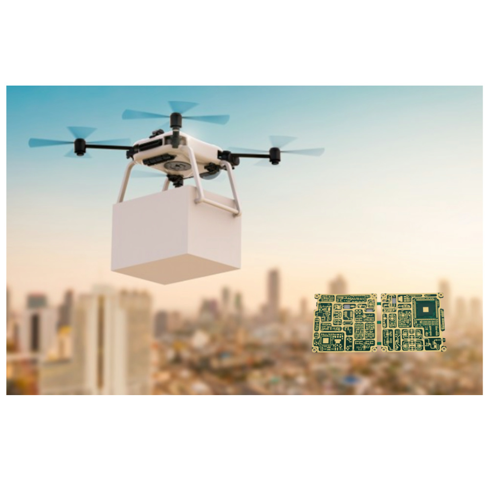
Deep Dive into RF PCB Design: From Fundamentals to Cutting-Edge Innovations
As a professional team deeply rooted in PCB design, Rich Full Joy has been committed to delivering top-tier technology and solutions for the industry. In this article, we provide a comprehensive analysis of RF PCB design, sharing our extensive experience and insights into advanced techniques for PCB engineers.
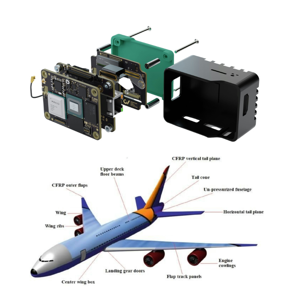
PCB Vias: Key Challenges and Solutions for High-Speed Signal Transmission
In printed circuit board (PCB) design and manufacturing, vias serve as crucial interconnects between different PCB layers. Despite their small size, they significantly impact electrical performance, particularly in high-speed signal transmission. As electronic devices continue evolving toward higher speeds and performance, mastering PCB via design and its effects on high-speed signals has become a critical challenge for PCB engineers and designers.
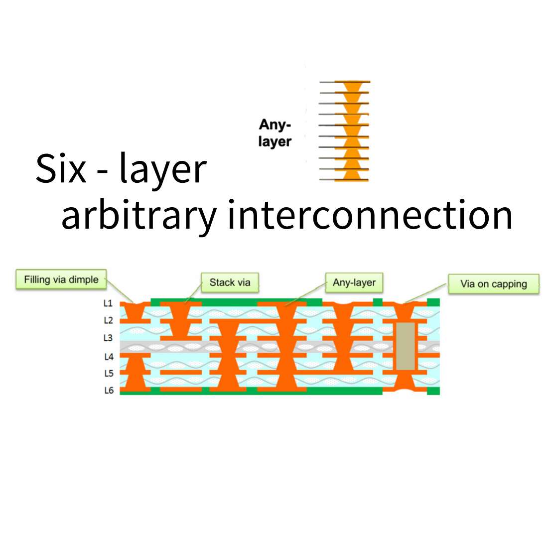
Insight into Common HDI Circuit Board Types and Their Applications | Rich Full Joy-1
Discover the key types of HDI circuit boards, including 1+N+1 and 3+N+3 layers, 10+N+10 layers and their applications in various industries. Learn how Rich Full Joy provides high-quality HDI PCB solutions for advanced electronics.

Exploring New Horizons in HDI Design: 3D Packaging and Heterogeneous Integration
Discover how 3D packaging and heterogeneous integration are transforming HDI PCB design. Learn about TSV technology, thermal management, electrical compatibility, and material selection to optimize high-performance electronic systems.

Unlocking the HDI Design Code: The Crucial Impact of Micro-Via and Blind-Via Designs on Performance
Explore the critical role of micro-via and blind-via designs in HDI PCB performance. Learn how precise via design enhances signal integrity, reduces EMI, and optimizes circuit density for advanced applications.
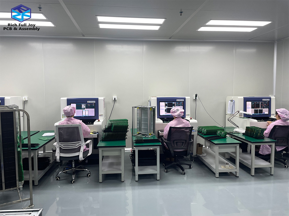
What is the difference between AOI and SPI20240904
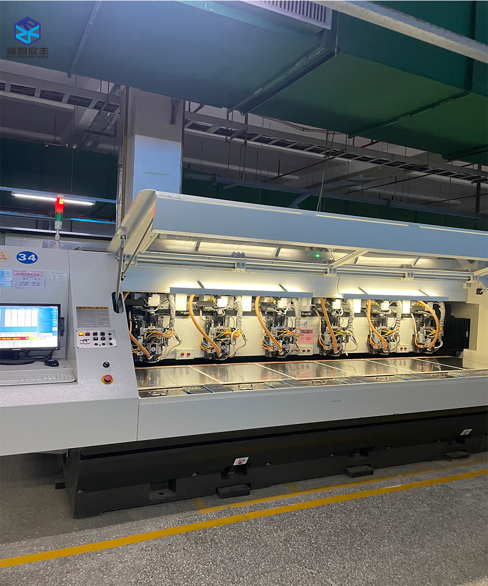
Controlled Depth Drilling in PCB Manufacturing: Back Drilling what is back drilling in pcb?
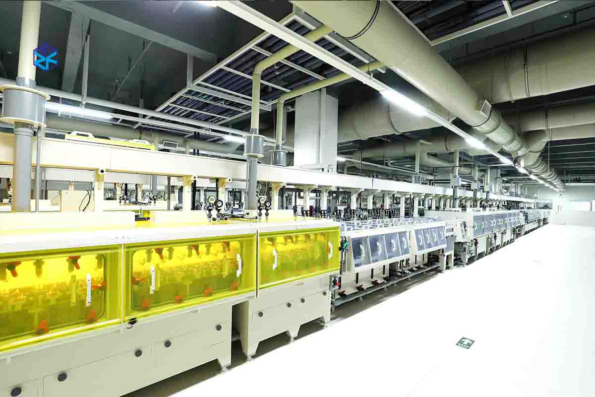
PCB Circuit Etching - Vacuum Etching Machine
The vacuum etching machine equipment uses chemical solutions to etch circuit patterns onto the PCB copper surface.
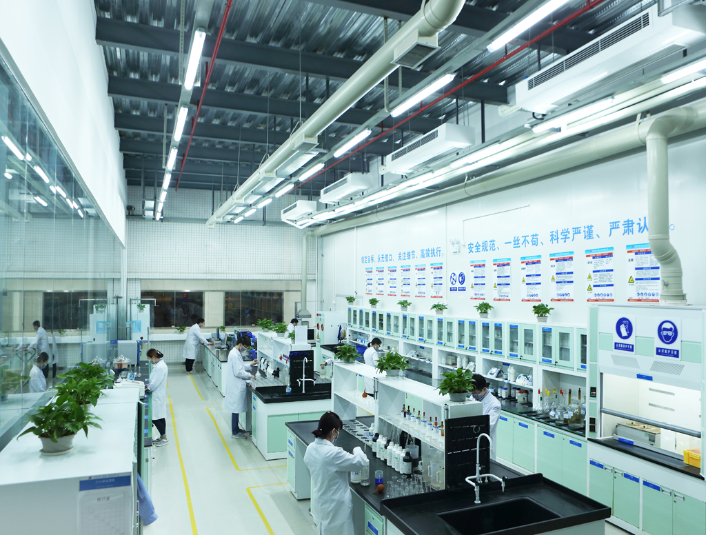
PCB Chemical Laboratory PCB Physical Laboratory World-Class Quality Assurance
Our team consists of experienced professionals with deep technical expertise in PCB manufacturing and testing. We offer a wide range of testing services, including material analysis, corrosion testing, electroplating, and surface treatment analysis. Whether it is multi-layer PCBs, high-frequency PCBs, or rigid-flex PCBs, we perform comprehensive quality evaluations to help clients optimize product performance and reliability.
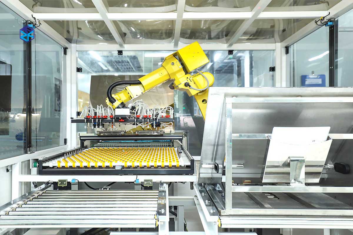
Automated PCB Loading and Unloading
To achieve automation and high-efficiency production, Shenzhen Rich Full Joy Electronics Co., Ltd. has introduced a Robotic PCB Handling System. This intelligent device replaces traditional manual operations by automating the Automated PCB Loading and Unloading processes, significantly enhancing production efficiency, product quality, and the level of Intelligent PCB Manufacturing Equipment within the enterprise.