











Unlocking the HDI Design Code: The Crucial Impact of Micro-Via and Blind-Via Designs on Performance
Unlocking the HDI Design Code: The Crucial Impact of Micro - via and Blind - via Designs on Performance
In the complex field of HDI (High - Density Interconnect) circuit board design, micro - via and blind - via designs are like the crucial codes hidden in the circuit maze, playing a decisive role in the performance of the circuit board. For engineers dedicated to HDI design, deeply understanding and precisely applying these two design elements is the core to breaking through design bottlenecks and achieving excellent performance.

1.Micro - via Design: The Fine Channel to High - Performance
(1) The Impact of Micro - via Size and Density on Electrical Performance
Micro - vias, as the fine channels connecting circuit lines on different layers of the circuit board, the selection of their size and density is directly related to the electrical performance of the circuit board. In application scenarios of ultra - high - speed signal transmission, such as the PCI - Express 6.0 interface with a signal rate as high as 64Gbps, the parasitic capacitance and inductance of micro - vias become key factors affecting signal integrity. According to electromagnetic theory, the parasitic capacitance of micro - vias is proportional to the square of the via diameter, and the parasitic inductance is proportional to the via depth. Therefore, using smaller - sized micro - vias (such as 50μm or even smaller) can significantly reduce parasitic capacitance and decrease the delay and attenuation during signal transmission. At the same time, reasonably increasing the density of micro - vias to achieve more efficient electrical connections within the limited circuit board space helps to improve signal transmission efficiency and meet the stringent requirements of high - speed data transmission for line density.
(2) The Selection and Optimization of Micro - via Processing Technology
The accuracy and quality of micro - via processing technology directly determine the performance of micro - vias. Currently, mainstream micro - via processing technologies include laser drilling, plasma etching, etc. Laser drilling technology, with its advantages of high precision and high flexibility, is widely used in the manufacturing of HDI circuit boards. When using the laser drilling process, engineers need to precisely control parameters such as the energy, pulse width, and focus position of the laser. For example, excessive laser energy may cause carbonization of the hole wall, increasing resistance and affecting signal transmission; inaccurate pulse width and focus position may lead to size deviations and irregular shapes of micro - vias. By optimizing these parameters and combining advanced drilling equipment and an automated control system, high - precision processing of micro - vias can be achieved, ensuring smooth hole walls without burrs, thereby improving the reliability and electrical performance of micro - vias.
2.Blind - via Design: The Key Strategy to Improve Signal Integrity
(1) The Matching of Blind - via Types and Application Scenarios
Blind - vias can be divided into top - layer blind - vias, bottom - layer blind - vias, and middle - layer blind - vias according to their positions and connection methods in the circuit board. Different types of blind - vias are suitable for different application scenarios. In designs with extremely high requirements for space size and signal transmission quality, such as smartphone motherboards, top - layer blind - vias and bottom - layer blind - vias can effectively reduce the number of vias on the circuit board surface, reduce signal interference, and at the same time achieve efficient connection between surface components and inner - layer lines. In multi - layer board designs, middle - layer blind - vias are often used to connect signal lines in the middle layer, optimize the signal transmission path, and reduce the transmission loss of signals inside the circuit board. For example, in the design of high - end server motherboards, through the reasonable use of middle - layer blind - vias, the signals of different functional modules can be effectively isolated, signal crosstalk can be avoided, and the stability and reliability of the system can be improved.
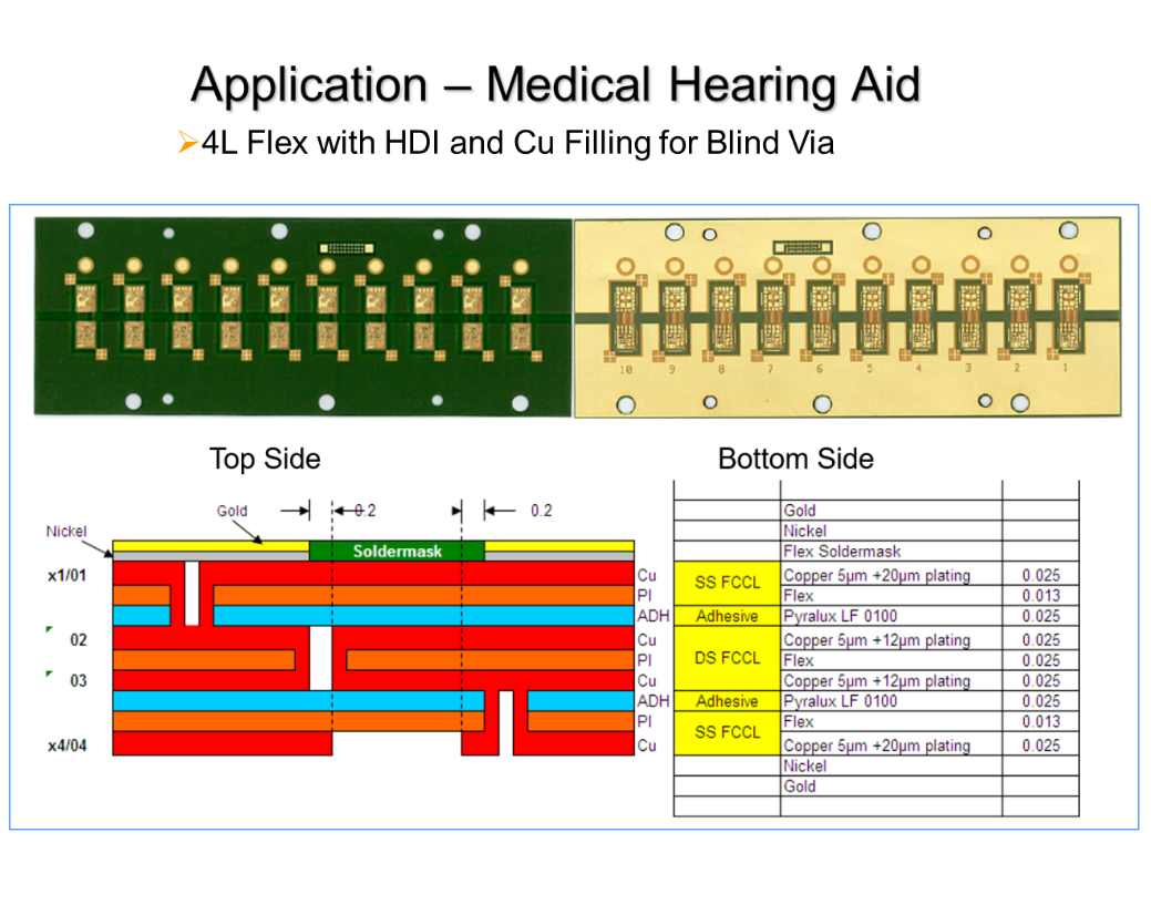
(2) The Optimization of Signal Integrity by Blind - via Design
Blind - via design has significant advantages in improving signal integrity. Compared with through - vias, blind - vias can reduce the reflection and scattering of signals at the vias and lower the signal transmission loss. This is because blind - vias only connect part of the layers of the circuit board, avoiding the signal passing through too many dielectric layers in the through - via, thus reducing the interaction between the signal and the surrounding medium. In high - speed digital circuit design, signal integrity is the key to ensuring system performance. By reasonably designing the position, size, and number of blind - vias and combining precise impedance control technology, signal reflection and crosstalk can be effectively reduced, ensuring the stable transmission of signals on the circuit board. For example, when designing a high - speed serial interface circuit, arranging blind - vias at key positions on the signal transmission path and optimizing the matching between the size of the blind - vias and the lines can significantly improve the signal - to - noise ratio of the signal and enhance the accuracy and reliability of data transmission.
3.The Cooperative Optimization of Micro - via and Blind - via Designs
(1) Design Considerations Based on Overall Performance
In actual HDI design, micro - vias and blind - vias do not exist in isolation but need to work together to optimize the overall performance of the circuit board. Engineers should start from the overall functional requirements of the circuit board, comprehensively consider factors such as signal transmission paths, power distribution networks, and heat dissipation requirements, and reasonably plan the layout of micro - vias and blind - vias. For example, when designing a high - frequency circuit, in order to reduce signal transmission loss, micro - vias and blind - vias should be preferentially arranged on the shortest signal transmission path and ensure that their connection with the lines has good electrical performance. At the same time, in the design of power and ground layers, the rational use of micro - vias and blind - vias to optimize the distribution of power and ground can effectively reduce the interference of power noise on signals and improve the stability of the system.
(2) Simulation and Verification in the Design Process
Due to the complex impact of micro - via and blind - via designs on the performance of the circuit board, relying solely on experience for design often fails to achieve the best results. Therefore, in the design process, it is crucial to use advanced Electronic Design Automation (EDA) tools for simulation and verification. Through 3D electromagnetic field simulation software such as HFSS and CST, engineers can accurately simulate the electrical performance of micro - vias and blind - vias at different frequencies, including parasitic parameters, signal transmission loss, and crosstalk. According to the simulation results, optimizing and adjusting the design can help discover and solve potential problems before actual manufacturing, improving the success rate and efficiency of the design. For example, when designing a new HDI circuit board, through simulation analysis, it is found that the blind - via design in a certain area causes excessive signal crosstalk. Engineers can effectively reduce crosstalk and ensure signal integrity by adjusting the position, size of the blind - vias, or adding shielding measures.

Rich Full Joy is a leading figure in the HDI manufacturing field. With its profound technical precipitation and continuous innovation investment, it demonstrates extraordinary professionalism in micro - via and blind - via designs and manufacturing processes. Taking the HDI circuit board of 5G base stations as an example, Rich Full Joy has greatly improved the attenuation and interference problems of signals during high - frequency band transmission by optimizing micro - via and blind - via designs, making the 5G signal coverage wider and the transmission rate more stable, and effectively enhancing the communication quality. In the manufacturing of HDI circuit boards for high - end servers, Rich Full Joy uses advanced micro - via processing technology and blind - via layout schemes to solve the data transmission error problem caused by signal crosstalk, significantly improving the stability of server operation and data processing efficiency, and providing a solid hardware foundation guarantee for enterprise - level applications. These achievements not only demonstrate the excellent strength of Rich Full Joy in HDI manufacturing but also provide strong support for the upgrading of electronic products in various industries, becoming a trusted partner for many HDI design engineers.









