











High-Frequency RF PCBs: The Core Power of Wireless Communication
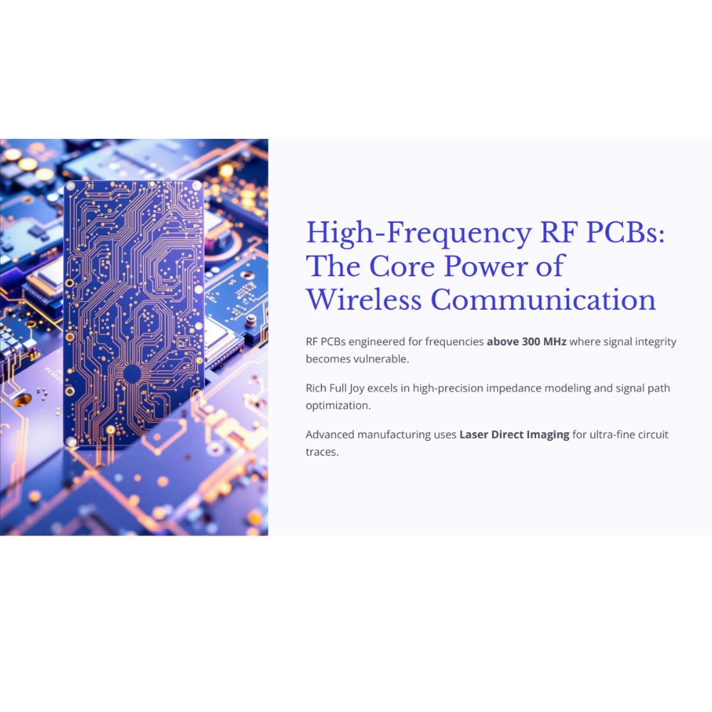
RF PCBs are engineered to handle radio frequencies typically above 300 MHz. At such high speeds, signal integrity becomes extremely vulnerable to interference and loss, making design and fabrication a high-stakes challenge. This is where Rich Full Joy stands out.
During the design phase, accurate impedance matching is essential to maintain signal stability. Rich Full Joy’s engineering team utilizes proprietary high-precision impedance modeling, combined with advanced simulation tools, to calculate and fine-tune circuit impedance. Even in complex board layouts, the impedance tolerance is tightly controlled to reduce reflections and preserve signal fidelity.
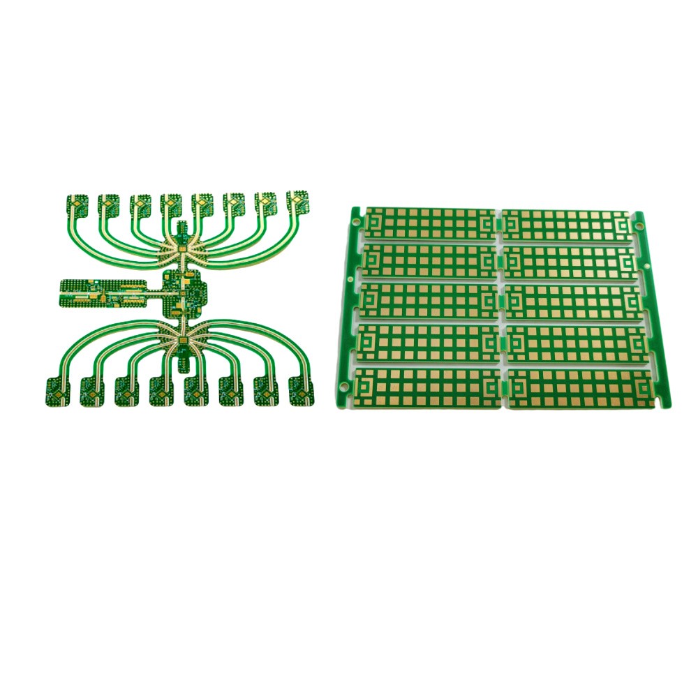
Signal path optimization is equally vital. Given the shorter wavelengths of high-frequency signals, any discontinuity in the path can trigger interference. Rich Full Joy engineers meticulously lay out each trace to minimize signal path length and reduce transmission loss. Microstrip, stripline, and other transmission line techniques are used to maintain stable propagation characteristics.
In manufacturing, Rich Full Joy adopts cutting-edge processes. Laser Direct Imaging (LDI) is used to define ultra-fine circuit traces with high resolution, ensuring compliance with high-frequency performance demands. In multilayer board fabrication, their advanced lamination process precisely controls temperature, pressure, and dwell time, resulting in tightly bonded layers that suppress interlayer crosstalk and enhance mechanical strength.
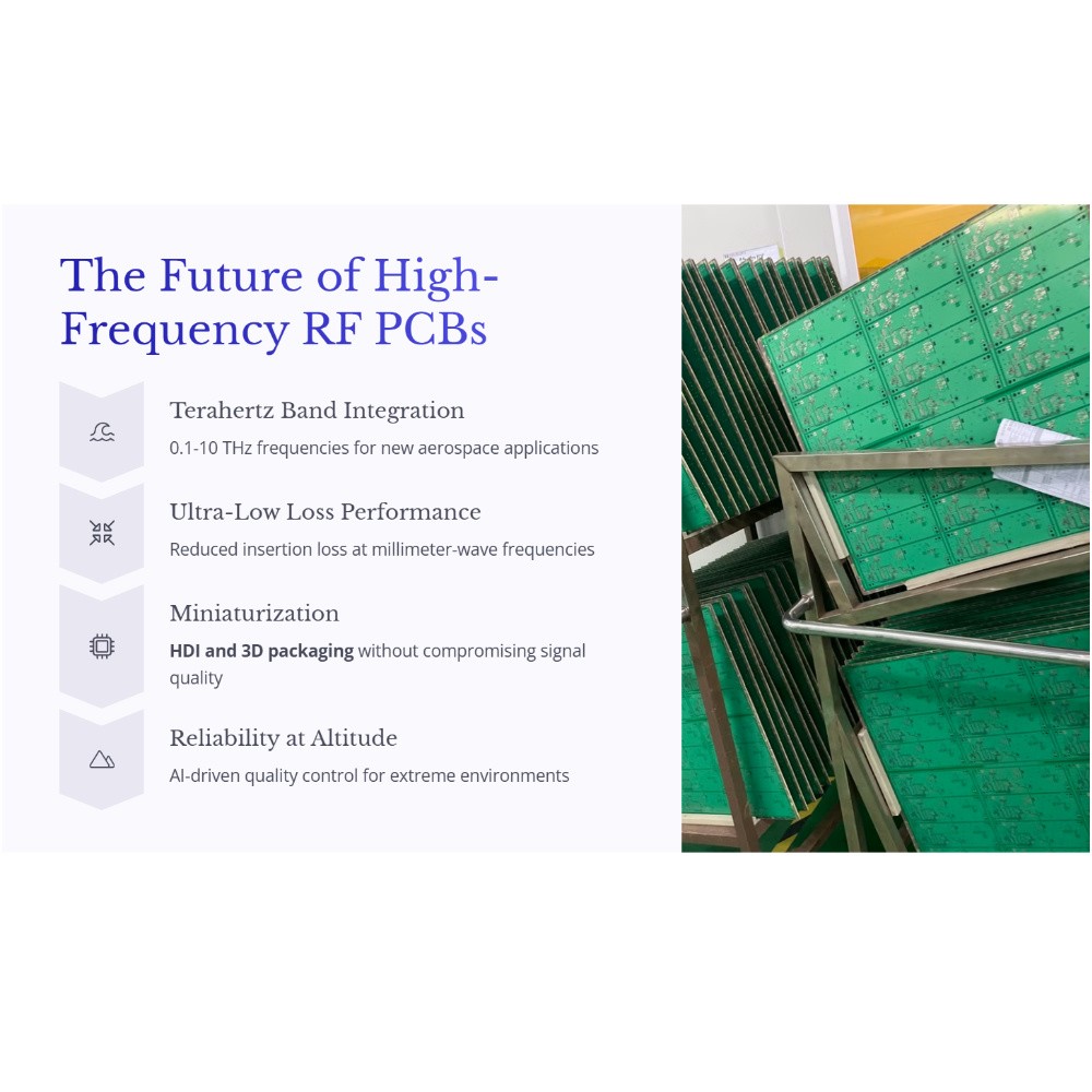
When working with specialty materials such as PTFE composites, Rich Full Joy’s experience makes the difference. PTFE is known for its excellent dielectric properties but also poses fabrication challenges like warpage and poor adhesion. Rich Full Joy has mastered these materials, applying proprietary techniques that maintain the structural and electrical integrity of the board.
RF PCBs in Aerospace: Rich Full Joy’s Unmatched Performance
The aerospace industry imposes the most demanding conditions on RF PCB design and production. Rich Full Joy has developed a suite of solutions specifically tailored to meet these challenges.
In material selection, aerospace-grade RF PCBs must exhibit high dielectric stability, low loss, and excellent thermal performance. Rich Full Joy not only utilizes PTFE composites but also leverages advanced ceramic-filled laminates. These materials are thoroughly evaluated across multiple dimensions—including dielectric performance, thermal behavior, and mechanical strength—using Rich Full Joy’s proprietary screening methodology.

To unlock the full performance potential of these materials, Rich Full Joy has optimized drill and surface preparation methods to prevent issues such as delamination or cracking, enhancing the adhesion between layers and improving electrical connectivity.
In terms of EMC and shielding design, the company anticipates the complex electromagnetic environment of aircraft systems. Techniques such as embedded ground planes, shielding vias, and metal cans are integrated into the design to isolate critical signal paths from external interference.
Tolerances on drill diameters, trace width, and spacing are tightly controlled using state-of-the-art drilling and photolithography systems. Rich Full Joy ensures every board is within the narrowest possible deviation band to maintain consistency in signal behavior across the fleet.
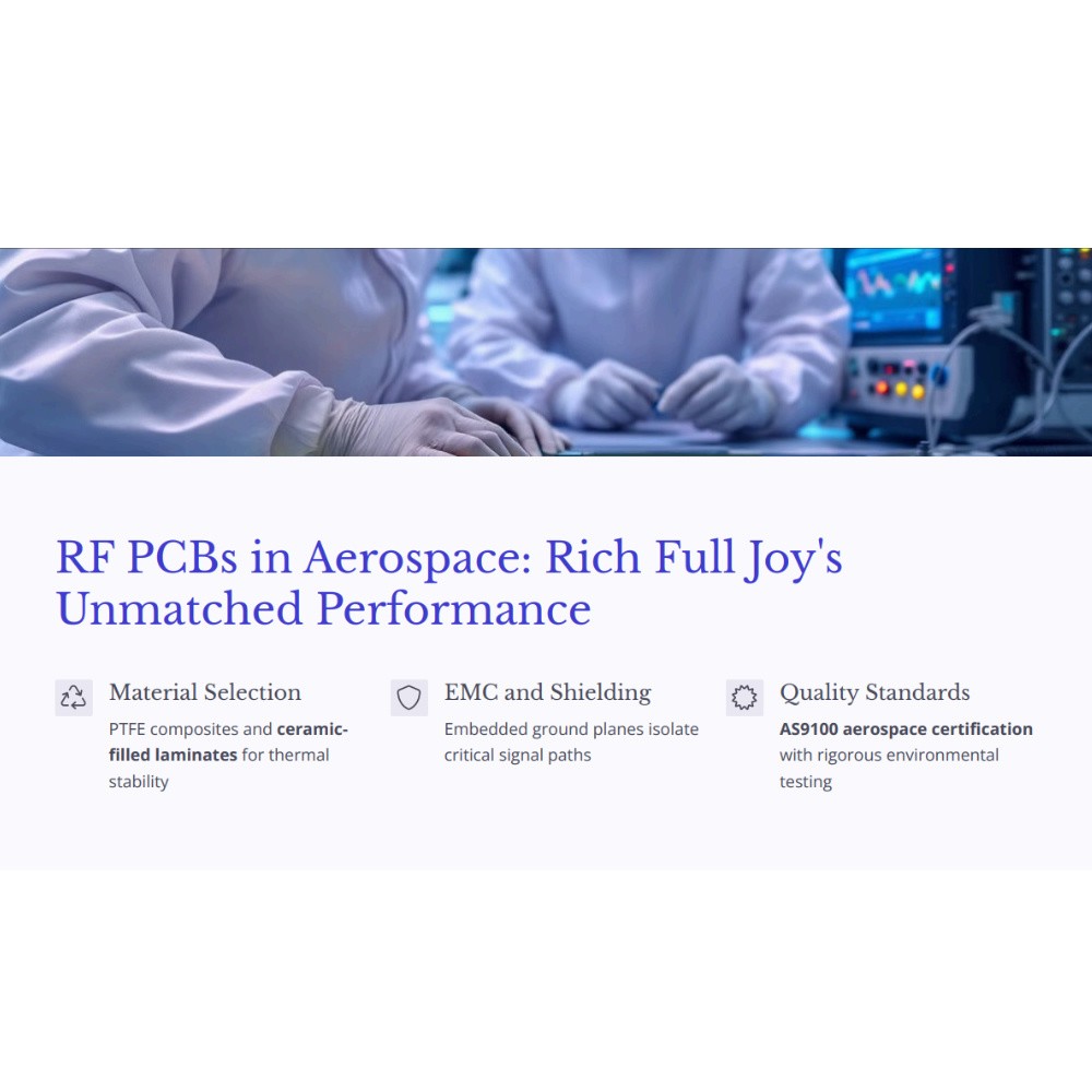
Critically, Rich Full Joy adheres to AS9100 aerospace quality standards, establishing a comprehensive quality system that spans raw material inspection, in-process quality checks, and end-of-line testing. Each RF PCB is subject to rigorous environmental testing, including thermal cycling, vibration, low-pressure simulation, and radiation resistance to simulate aerospace conditions.
Widespread Applications of RF PCBs in Aerospace Systems
Rich Full Joy’s high-frequency RF PCBs power essential systems in modern aircraft, including:
●Communication systems that demand real-time data, voice, and video transmission
●Navigation systems like GPS and INS that require precise signal processing
●Radar systems, including phased-array radars that rely on high-frequency RF boards for wide-area surveillance and target tracking
These applications demand ultra-reliable, low-loss, and interference-resistant PCBs, all of which are hallmarks of Rich Full Joy’s design philosophy.
The Future of High-Frequency RF PCBs
Looking ahead, RF PCBs will face even more ambitious technical demands:
●Terahertz Band Integration: Rich Full Joy is investing in research collaborations to develop materials and processes that support frequencies from 0.1 THz to 10 THz, opening new frontiers in aerospace communication and imaging.
●Ultra-Low Loss Performance: Through advanced material engineering and signal path optimization, Rich Full Joy is reducing insertion loss even at millimeter-wave frequencies.
●Miniaturization and HDI: With increasing demand for lighter and smaller electronics in aircraft, Rich Full Joy applies HDI and 3D packaging to condense functionality without compromising signal quality.
●Reliability at Altitude: Enhanced fault detection, predictive analytics, and AI-driven quality control are being used to ensure boards maintain performance in extreme environments.
Why Choose Rich Full Joy
With world-class engineering capabilities, deep aerospace domain knowledge, and a relentless commitment to innovation, Rich Full Joy is the trusted partner for mission-critical high-frequency RF PCB manufacturing. Whether for commercial aircraft, satellites, or defense-grade systems, Rich Full Joy delivers uncompromising quality, performance, and technical support.
Industry Professionals, Are You Ready to Solve These Challenges?
✓ How do you master RF PCB design fundamentals?
✓ Why is multilayer RF PCB yield so difficult to improve?
✓ How do surface treatments affect long-term performance?
✓ What does it take to meet international RF PCB quality standards?
Coming Soon on LinkedIn – Don’t miss this expert-level knowledge series:LinkedIn
April 11 – RF PCB Design Mastery from Theory to Real-World Deployment
April 14 – Multilayer RF PCB Manufacturing and Lamination Control
April 16 – Surface Treatment Optimization for RF PCB Solderability
April 18 – Interpreting RF PCB Quality Standards Like a Pro
Join us to unlock exclusive white papers, engage in technical Q&A, and elevate your RF engineering expertise.









