Why High-Frequency PCB Insertion Loss Is Still Out of Control
Why Does Insertion Loss Remain a Critical Barrier in High-Frequency PCB Design?
Insertion loss in high-frequency PCBs continues to be one of the most underestimated yet dominant factors limiting system performance in 5G, radar, and millimeter-wave applications.
As operating frequencies move beyond multi-GHz into mmWave bands, even minor discontinuities in transmission paths result in measurable signal degradation.
Key reasons insertion loss remains difficult to control include:
• Frequency-dependent dielectric loss scaling exponentially at mmWave range
• Copper surface roughness increasing effective RF resistance
• Via discontinuities introducing reflection and energy leakage
• Stack-up inconsistencies affecting impedance continuity
• Material variability under thermal and manufacturing stress
In modern RF systems, insertion loss is no longer just a design parameter—it is a system-level performance limiter.
How Do High-Frequency Materials Influence Insertion Loss Behavior?

Material selection is the first and most critical determinant of insertion loss behavior in RF PCBs.
High-frequency laminates such as low-loss hydrocarbon ceramic systems are designed to minimize dielectric dissipation, but real-world manufacturing introduces variability.
Engineering factors include:
• Dielectric constant (Dk) stability across frequency bands
• Dissipation factor (Df) behavior under GHz excitation
• Moisture absorption effects on RF propagation
• Resin-glass fiber interface scattering effects
Even small Df deviations (0.002–0.005 range) can significantly amplify insertion loss at 20–40 GHz applications.
Material inconsistency across production batches further worsens predictability in mass production environments.
Why Does Copper Surface Roughness Increase Signal Loss in RF PCBs?
At high frequency, current does not flow uniformly through copper—it concentrates at the surface due to skin effect.
This makes copper surface topology a major contributor to insertion loss.
Key mechanisms include:
• Increased effective path length due to microscopic roughness
• Signal scattering at copper-laminate interfaces
• Higher RF resistance at skin depth scale
• Manufacturing-induced etching inconsistencies
Even "low-profile copper" still introduces measurable degradation in mmWave bands.
In practical RF design, copper roughness can account for a significant portion of total insertion loss beyond 10 GHz.
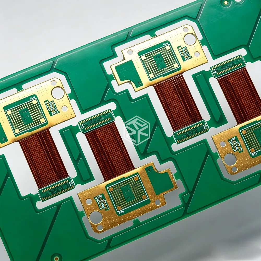
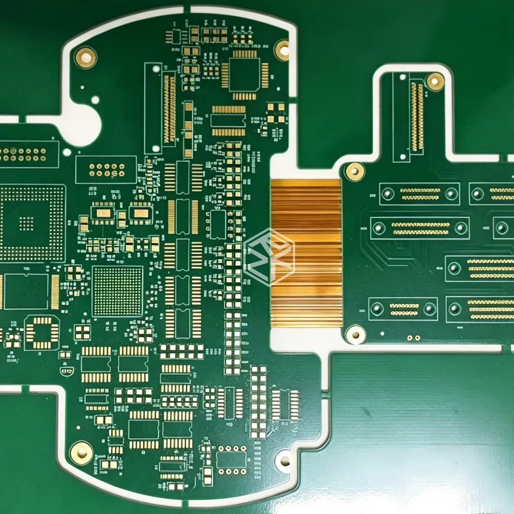
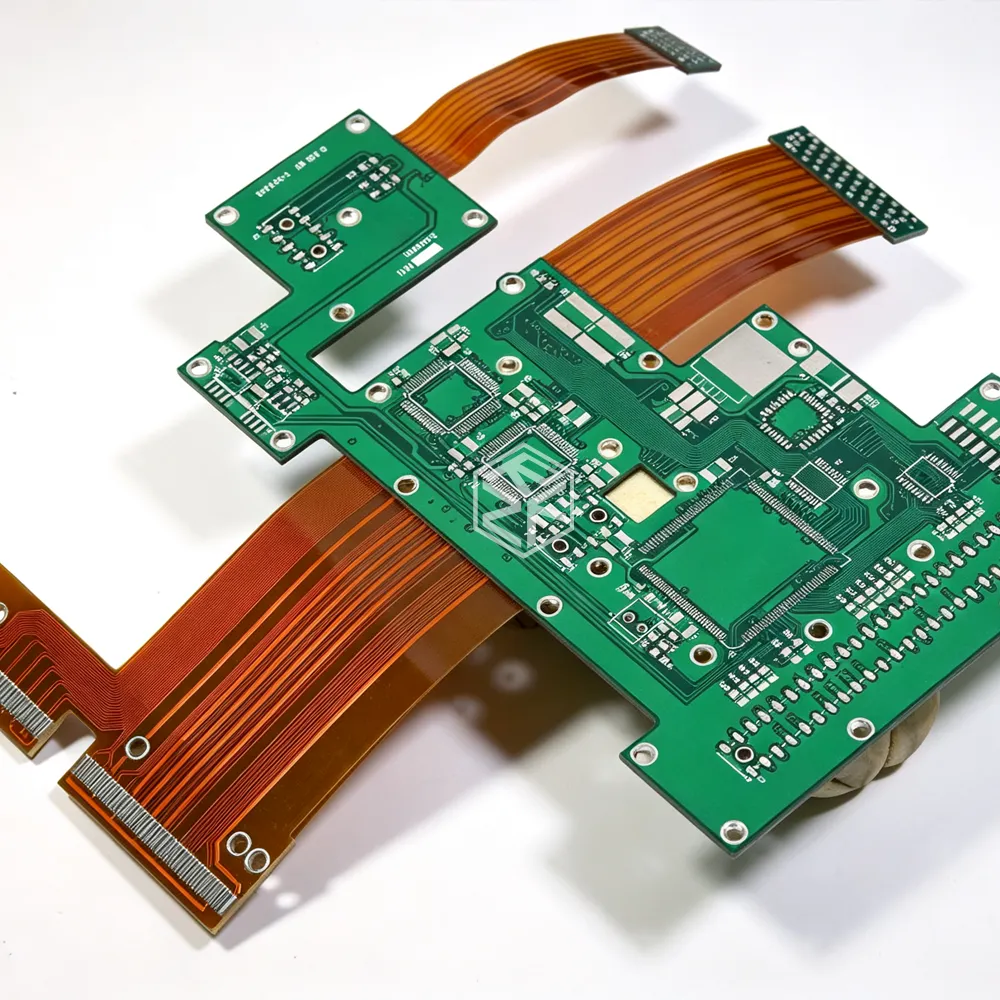
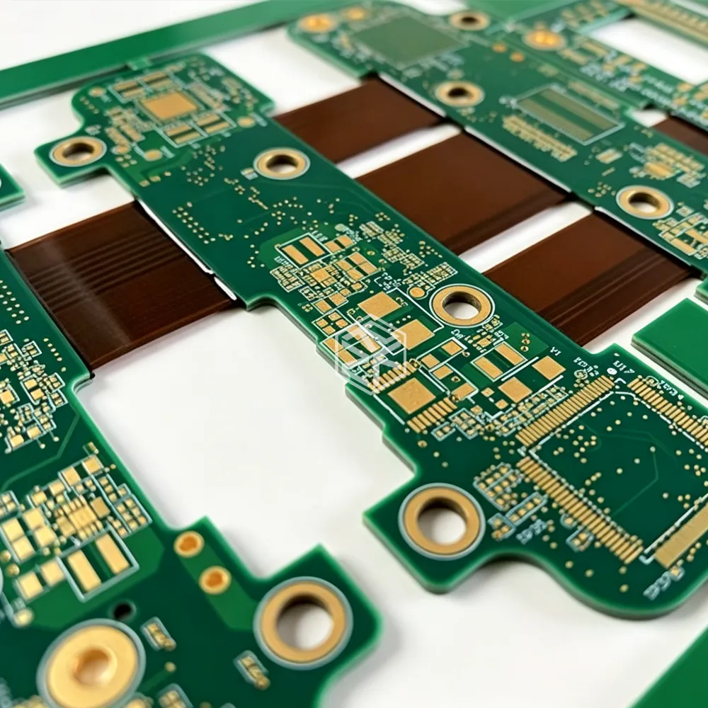
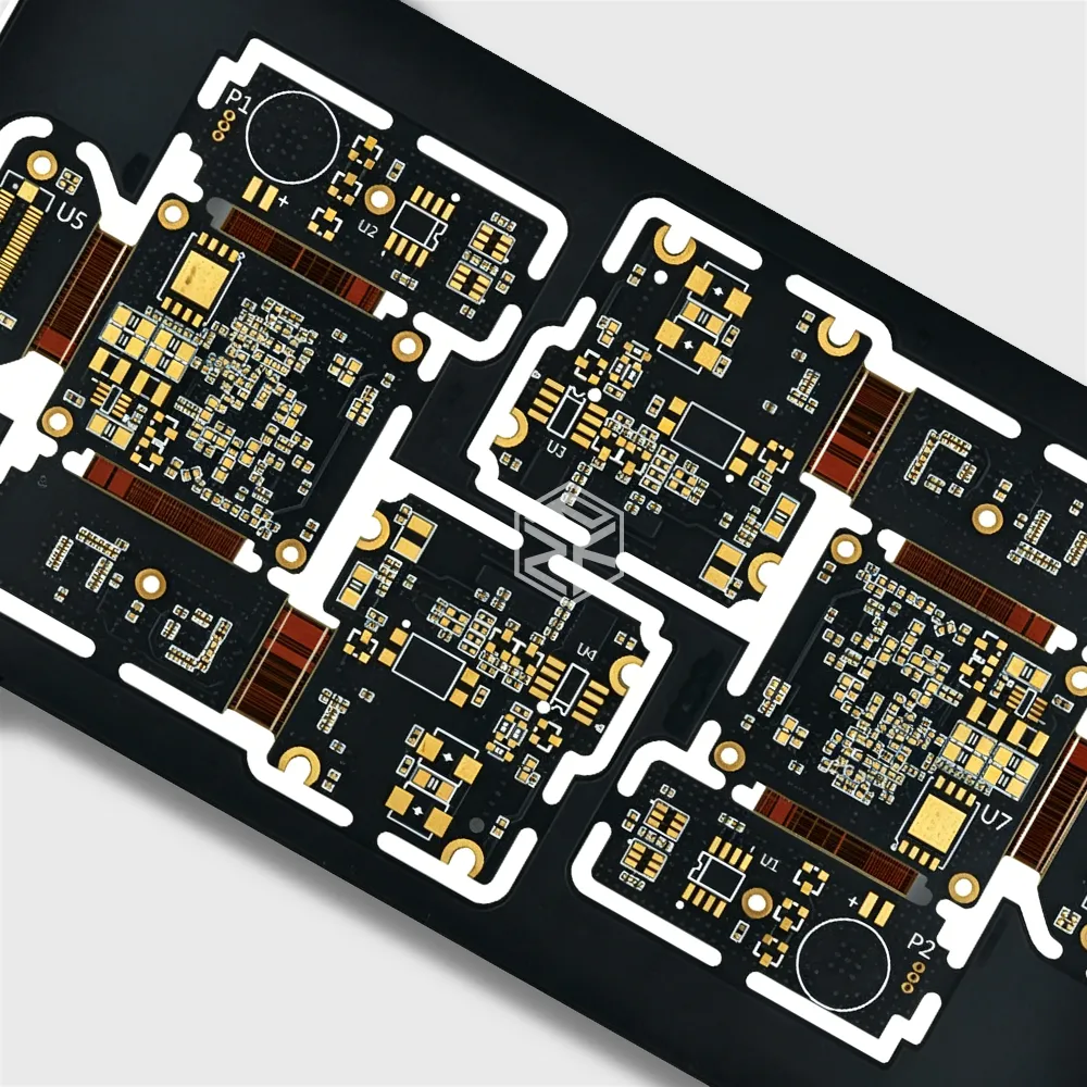
How Do Via Structures and HDI Design Amplify Insertion Loss?
High-density interconnect (HDI) structures are essential for modern compact RF modules but also introduce additional loss mechanisms.
Critical via-related issues include:
• Via stubs causing resonant signal reflections
• Impedance discontinuity in layer transitions
• Electromagnetic field leakage in via barrels
• Back-drill tolerance variation affecting signal integrity
Microvia stacking and staggered via designs help reduce these effects, but each transition still introduces measurable insertion loss at high frequency.
As frequencies increase, via optimization becomes a dominant RF engineering constraint rather than a layout convenience.
Why Does Impedance Mismatch Still Happen in Controlled Impedance Designs?

Even in "controlled impedance" PCB designs, real-world manufacturing variation creates mismatch conditions that contribute to insertion loss.
Root causes include:
• Etching tolerance variations altering trace width
• Dielectric thickness deviation during lamination
• Resin flow inconsistency in hybrid stack-ups
• Reference plane discontinuities in multilayer routing
A nominal 50Ω design can easily drift beyond tolerance under thermal or fabrication variation, causing energy reflection and increased insertion loss.
This is especially critical in differential high-speed RF channels.
How Does Thermal Stress Increase Insertion Loss Over Time?
Thermal cycling introduces mechanical and electrical instability in RF PCBs.
Key degradation mechanisms include:
• Expansion mismatch between copper and dielectric layers
• Micro-cracking in vias and interconnects
• Drift in dielectric constant under temperature load
• Long-term material aging affecting RF performance
Over time, insertion loss does not remain static—it degrades progressively under operational stress.
This is especially visible in base station and aerospace applications where continuous thermal cycling is unavoidable.
What Engineering Techniques Can Reduce Insertion Loss?
Reducing insertion loss requires a system-level RF engineering approach rather than isolated material selection.
Key mitigation strategies include:
• Optimized stack-up design for field containment
• Back-drilling to eliminate via stubs
• Smooth copper or reverse-treated foils for RF layers
• Differential pair length matching for phase consistency
• Ground stitching vias for EMI suppression
• Hybrid dielectric structures for RF/digital isolation
Simulation-driven design (HFSS, CST, ADS) combined with manufacturing feedback loops is essential to stabilize performance.
Why Is Manufacturing Control the Missing Link in Loss Optimization?
Even the best RF design can fail if manufacturing control is not precise.
Critical process controls include:
• Lamination pressure uniformity
• Drill accuracy for microvias
• Plasma desmear consistency
• Impedance coupon verification (TDR testing)
• Copper plating thickness control
Insertion loss is not purely a design issue—it is a fabrication repeatability issue.
This is why RF PCB performance often varies between prototype and mass production.
Applications Where Insertion Loss Becomes Mission-Critical
High-frequency insertion loss directly impacts system-level performance in:
• 5G base station AAU/RRU modules
• Millimeter-wave radar systems (77–81 GHz)
• Satellite communication payloads
• High-speed SerDes interconnects
• RF front-end phased array antennas
• Automotive ADAS sensing modules
In these systems, even 0.5–1 dB loss variation can significantly degrade system sensitivity and range.
Frequently Asked Questions (FAQ)
What is insertion loss in high-frequency PCBs?
Insertion loss is the reduction of signal power as it travels through a PCB transmission path due to dielectric, conductor, and radiation losses.
Why does insertion loss increase at higher frequencies?
Because both dielectric loss and skin effect resistance increase with frequency, causing higher energy dissipation.
Can insertion loss be fully eliminated?
No. It can only be minimized through material selection, design optimization, and manufacturing control.
Which material helps reduce insertion loss?
Low-loss RF laminates with stable Dk/Df characteristics are commonly used in high-frequency applications.
Does HDI increase insertion loss?
HDI itself does not inherently increase loss, but via transitions and routing density can introduce additional discontinuities.
Conclusion: Why Insertion Loss Is Still Not Fully Controllable
High-frequency PCB insertion loss remains a persistent engineering challenge because it is influenced by multiple interacting variables—material physics, electromagnetic behavior, and manufacturing tolerances.
As systems move toward higher GHz and mmWave domains, insertion loss is no longer a secondary parameter—it is a system-level performance constraint that defines communication range, signal fidelity, and reliability.
Only a tightly integrated approach combining RF design, material science, and precision manufacturing can bring insertion loss under stable control.
Why Choose Rich Full Joy? Engineering-Driven RF PCB Manufacturing
Rich Full Joy provides advanced RF and high-speed PCB manufacturing solutions with deep engineering integration.
Core capabilities include:
• RF stack-up and impedance optimization
• Low-loss high-frequency material processing
• HDI and microvia precision manufacturing
• Controlled impedance validation and testing
• Prototype-to-mass production scalability
We focus on turning RF design challenges into manufacturable, stable, and repeatable production outcomes.