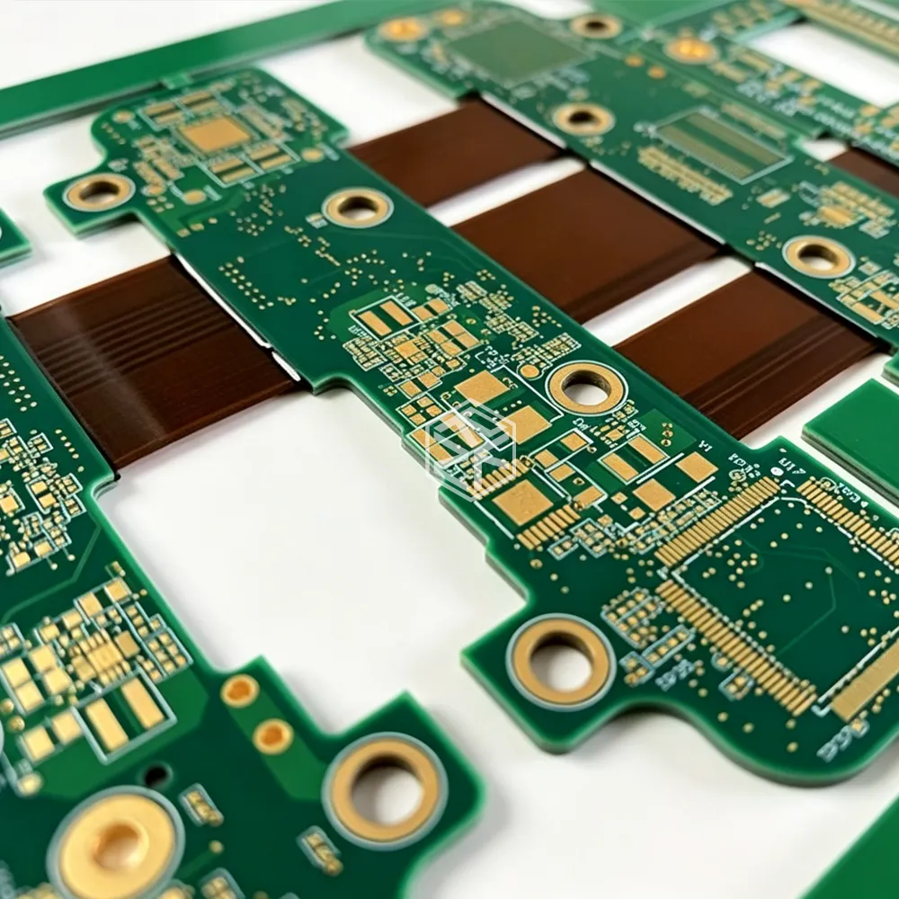
Plated Through Hole (PTH) Impact on RF Signal Integrity
Why Are Plated Through Holes No Longer “Passive” Structures in RF PCB Design?
In low-frequency electronics, plated through holes (PTHs) mainly function as simple electrical interconnects between PCB layers. However, in modern RF and high-speed systems operating above multi-GHz frequencies, PTHs become complex electromagnetic structures that directly influence signal integrity.
As frequencies rise, the electrical behavior of vias changes dramatically:
• Parasitic inductance increases
• Electromagnetic field discontinuity becomes more severe
• Reflection and insertion loss become measurable
• Return current paths become unstable
• Crosstalk and EMI risks increase
This means a via is no longer just a drilled conductive hole — it becomes part of the transmission line itself.
For 5G, radar, aerospace, and satellite communication systems, poor PTH optimization can severely degrade RF performance even when the transmission traces are correctly designed.
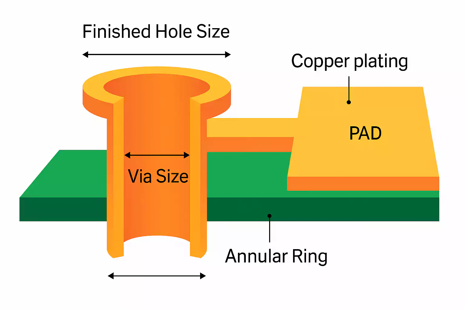
How Does PTH Geometry Affect RF Signal Integrity?
The physical dimensions of a plated through hole determine its high-frequency electrical behavior.
Critical parameters include:
• Drill diameter
• Via barrel depth
• Pad size
• Anti-pad clearance
• Copper plating thickness
• Layer transition distance
At high frequencies, signal energy becomes highly sensitive to any geometric discontinuity.
A large via barrel may increase capacitance, while insufficient anti-pad clearance can disturb electromagnetic field distribution. Excessive via depth also creates resonance risks.
In RF systems above 10 GHz, even micron-level dimensional variations can affect:
• Return loss
• Insertion loss
• Impedance continuity
• Phase stability
This is why RF PCB via engineering requires far tighter manufacturing tolerances than conventional PCB production.
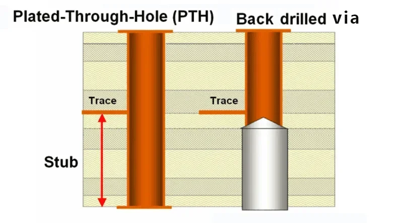
Why Do Via Stubs Become Dangerous at High Frequencies?
One of the most critical RF problems in multilayer PCBs is the via stub effect.
A via stub is the unused portion of a plated through hole extending beyond the active signal layer.
At low frequency, the impact may be negligible. But at high frequency, via stubs behave like resonant structures that store and reflect electromagnetic energy.
Consequences include:
• Signal reflection
• Increased insertion loss
• Eye-diagram degradation
• Phase distortion
• Resonance spikes at specific frequencies
The longer the via stub, the more severe the resonance effect becomes.
In modern 25G/56G/112G communication systems, uncontrolled via stubs can completely destroy channel performance margins.
How Does Back-Drilling Reduce RF Signal Loss?
Back-drilling is one of the most effective engineering solutions for reducing PTH-related signal degradation.
This process removes the unused via barrel section after plating, eliminating most of the stub structure.
Major RF advantages include:
• Reduced insertion loss
• Improved return loss
• Lower resonance risk
• Better differential signal quality
• Improved eye-diagram opening
Back-drilling is especially important in:
• 5G base station boards
• High-speed server backplanes
• RF front-end modules
• Aerospace communication hardware
• Millimeter-wave radar systems
Precise drill-depth control is critical because over-drilling may damage active conductive layers.
Why Is Return Current Stability Important Around PTH Structures?
RF current always travels in a complete electromagnetic loop. When a signal transitions through a via, the return current must also find a stable transition path.
Without nearby ground stitching vias:
• Return path inductance increases
• EMI radiation worsens
• Crosstalk becomes stronger
• Signal integrity degrades rapidly
This is why modern RF PCB layouts often surround signal vias with ground via fences.
Good return-path engineering significantly improves:
• Electromagnetic containment
• Differential pair stability
• Noise suppression
• High-frequency insertion loss performance
In RF systems, via placement strategy is just as important as trace routing itself.
How Do HDI and Microvia Structures Improve RF Performance?
Traditional PTH structures are increasingly replaced or supplemented by HDI microvia technology in advanced RF systems.
Microvias provide:
• Shorter signal transitions
• Lower parasitic inductance
• Reduced impedance discontinuity
• Higher routing density
• Better high-frequency field control
Stacked and staggered microvia structures are commonly used in:
• 5G antenna arrays
• Satellite RF modules
• Automotive radar systems
• AI accelerator communication boards
• High-density phased-array antennas
HDI technology is now considered essential for next-generation RF PCB manufacturing.
Real Engineering Case: 28GHz 5G Antenna Module Via Optimization
A telecommunications customer developing a 28GHz phased-array antenna module experienced severe insertion loss and unstable beamforming performance during prototype validation.
Initial issues included:
• High return loss near via transitions
• Differential signal skew
• Resonance peaks around 26–30 GHz
• Poor consistency between prototype batches
Engineering analysis identified several root causes:
• Excessive via stub length
• Inadequate ground via density
• Large anti-pad discontinuity
• Inconsistent via barrel plating thickness
Optimization actions included:
• Precision back-drilling
• Ground via fencing around RF transitions
• Reduced via stub depth
• HDI microvia transition redesign
• Improved copper plating process control
Results after optimization:
• Insertion loss improved by approximately 18%
• Return loss stability significantly improved
• Beamforming consistency increased across production panels
• RF channel reliability improved under thermal cycling
This case demonstrates how PTH optimization directly influences real-world RF system stability.
Applications Where PTH Optimization Is Mission-Critical
5G Base Stations
High-density RF routing and multi-layer transitions require precise via optimization to reduce insertion loss and maintain beamforming accuracy.
Automotive Radar Systems
77GHz radar modules are extremely sensitive to via discontinuity and impedance mismatch.
Satellite Communication Hardware
Long-duration thermal cycling demands highly reliable plated via structures with stable RF behavior.
Aerospace RF Electronics
Signal stability under vibration and temperature stress requires advanced via reliability engineering.
AI High-Speed Servers
112G PAM4 communication channels require ultra-low via reflection and precise impedance continuity.
Phased-Array Antenna Systems
Dense RF signal routing requires controlled via transitions and minimized electromagnetic coupling.
Why Manufacturing Quality Directly Determines RF Via Performance
Even the best RF layout design can fail if manufacturing consistency is poor.
Critical process control areas include:
• Laser drilling precision
• Copper plating uniformity
• Desmear process stability
• Lamination alignment accuracy
• Back-drill depth control
• AOI and X-ray inspection
At high frequencies, tiny manufacturing variations can produce measurable RF performance differences.
This is why RF PCB manufacturing requires a far more controlled engineering environment than standard PCB production.
Frequently Asked Questions (FAQ)
1. What is a plated through hole (PTH) in PCB manufacturing?
A PTH is a copper-plated drilled hole used to electrically connect multiple PCB layers.
2. Why do PTHs affect RF signal integrity?
Because vias introduce parasitic inductance and capacitance that disrupt high-frequency signal transmission.
3. What is a via stub?
A via stub is the unused portion of a via barrel extending beyond the active signal layer.
4. Why are via stubs harmful in RF systems?
They create resonance and reflection effects that increase insertion loss and degrade signal quality.
5. What is back-drilling?
Back-drilling removes unused via stub sections to improve high-frequency electrical performance.
6. Are microvias better than traditional PTHs for RF applications?
Yes. Microvias reduce parasitic effects and improve impedance continuity in high-frequency designs.
7. Why are ground vias important near signal vias?
Ground vias provide stable return current paths and reduce EMI and crosstalk.
8. How does copper plating quality affect RF performance?
Uneven plating changes via impedance and increases conductor loss at high frequencies.
9. Which applications are most sensitive to PTH design?
5G systems, radar modules, satellite communication hardware, and high-speed server boards.
10. How can RF via performance be validated?
Through TDR testing, S-parameter analysis, VNA measurements, and full-wave electromagnetic simulation.
Conclusion: PTH Engineering Is a Core RF Performance Factor
In modern high-frequency PCB systems, plated through holes are no longer secondary mechanical features — they are critical RF structures that directly determine signal integrity performance.
From via stub resonance and impedance discontinuity to return-path stability and EMI suppression, RF via engineering now plays a major role in:
• 5G communication systems
• Millimeter-wave radar
• Aerospace electronics
• Satellite communication
• High-speed AI computing hardware
Achieving stable RF performance requires deep integration between:
• Stackup engineering
• Via optimization
• HDI technology
• Back-drilling capability
• Precision manufacturing control
• RF simulation validation
As frequencies continue increasing, advanced PTH engineering will remain essential for next-generation RF PCB reliability and scalability.
Why Choose Rich Full Joy for RF PCB Manufacturing?
Rich Full Joy provides advanced RF PCB and high-frequency manufacturing solutions for demanding communication and microwave applications.
Our engineering capabilities include:
• Controlled impedance RF PCB fabrication
• HDI and microvia manufacturing
• Precision back-drilling technology
• RF stackup optimization
• High-frequency material processing
• Signal integrity verification and testing
• Prototype-to-volume production scalability
We help customers convert complex RF interconnect challenges into stable, manufacturable, and production-ready PCB solutions for next-generation communication systems.