Designing for Manufacturability in High-Frequency PCBs: Aligning Innovation with Production Reality
Introduction
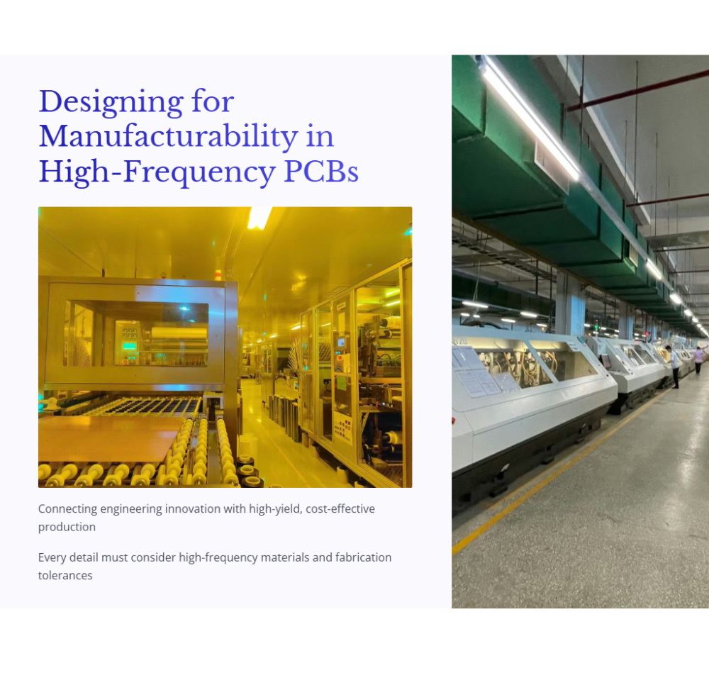
In the design of high-frequency PCBs, design for manufacturability (DFM) is the critical bridge that connects engineering innovation with high-yield, cost-effective production. For RF PCB design engineers, mastering DFM principles means creating boards that are not only functional but also reliable, scalable, and economically viable to produce.
From trace spacing to stackup structure, via design, and pad geometry, every detail must consider the realities of high-frequency materials and fabrication tolerances. This article outlines the essential elements of manufacturable high-frequency PCB design and how it impacts quality, efficiency, and cost.

1. Trace Design and Manufacturing Compatibility
Optimal Trace Width and Spacing
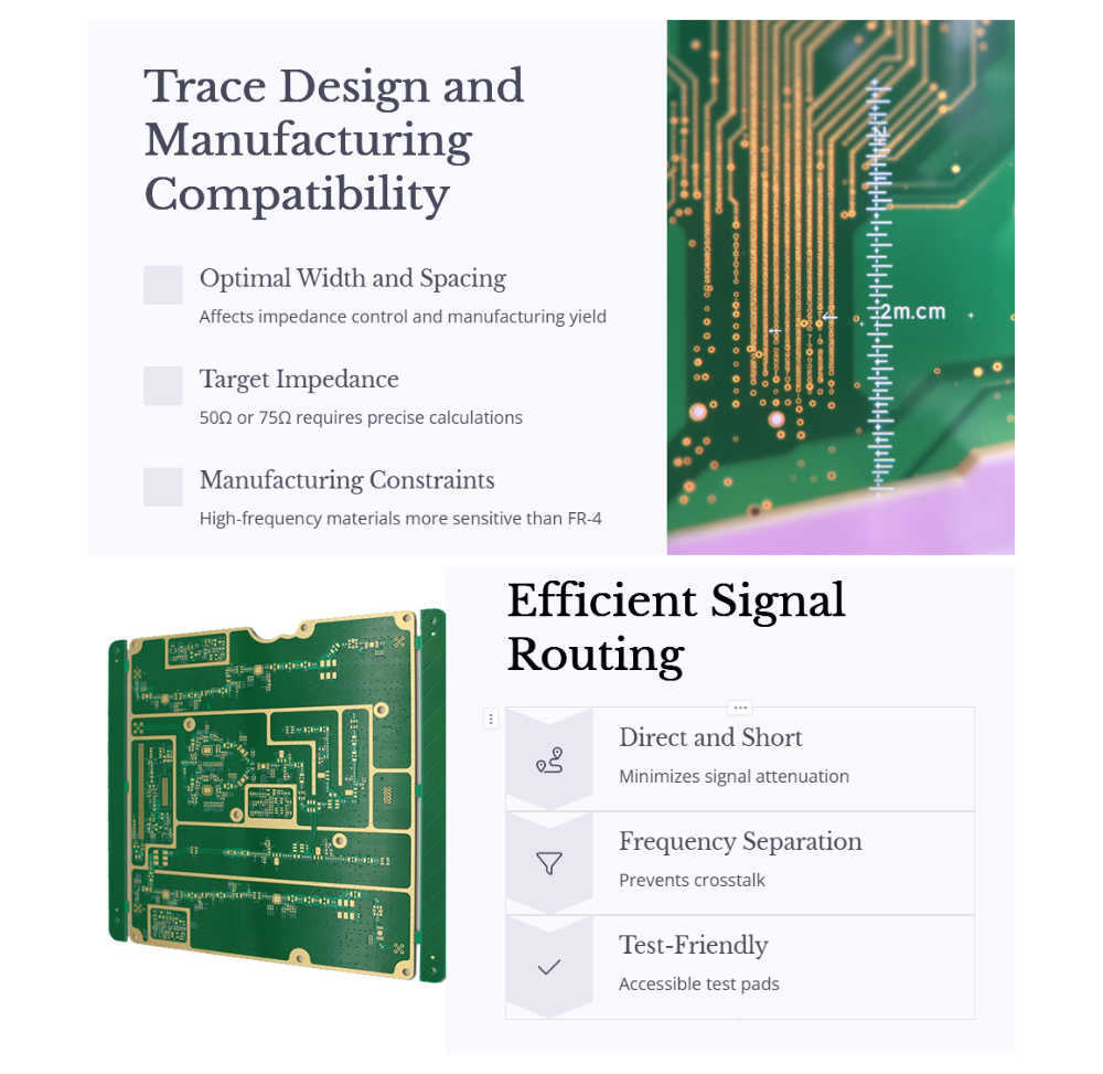
In high-frequency PCBs, trace width and spacing affect both electrical performance (e.g., impedance control) and manufacturing yield.
- Target impedance: 50Ω or 75Ω—requires precise trace width/spacings calculated using laminate Dk
- Manufacturing constraints: For high-frequency materials, process variation is more sensitive than with standard FR-4
Design Guideline: Avoid pushing the lower limit of etching tolerance. Instead of 3mil/3mil, use 4mil/4mil or larger on high-frequency laminates to prevent shorts, opens, or trace damage.
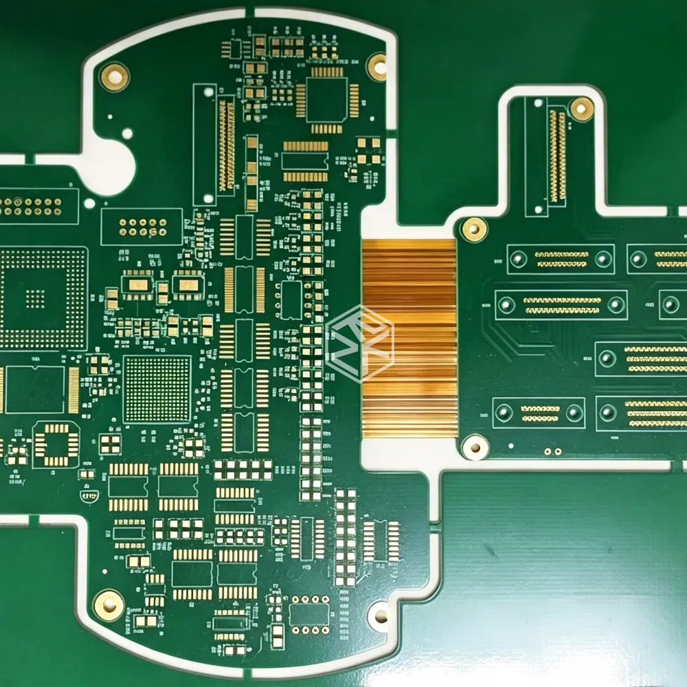
Efficient Signal Routing
Effective routing for high-speed signals should be:
- Direct and short (minimizing signal attenuation)
- Separated by frequency domain (preventing crosstalk)
- Test-friendly (with accessible test pads)
This improves signal integrity, supports production testing, and prevents functional defects during deployment.
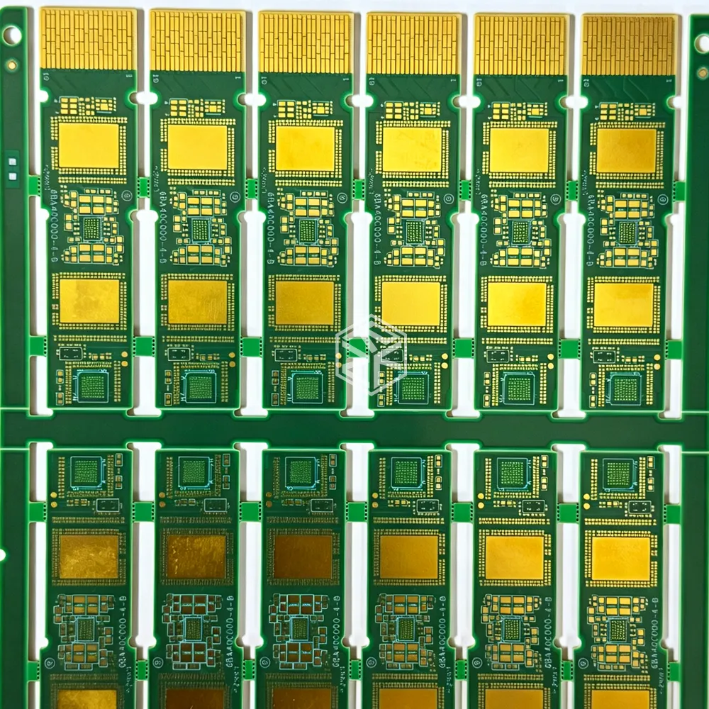
2. Stackup Structure: Balancing Electrical and Manufacturing Demands
Layer Count and Material Selection
- More layers = better signal/power separation, but higher cost and risk
- Too few layers = poor EMI control, compromised routing
For complex RF applications like 5G, 10+ layers are common. Rogers RO4350B is a popular choice for low Dk/Df needs, but it requires tighter control in processing.
Engineering Tip: Choose laminates not only for performance but also for their machinability, bonding behavior, and thermal stability during lamination.
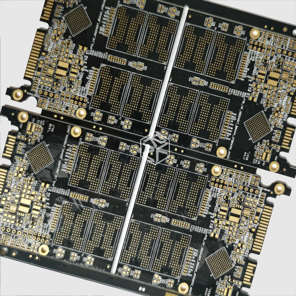
Lamination Process Considerations
Multilayer RF PCBs require tight control over:
- Registration accuracy (±50μm)
- Pressing parameters: 180–220°C, 5–10MPa, 30–60 min depending on prepreg and copper balance
Stackup optimization should balance dielectric distribution and copper symmetry to ensure even lamination and avoid warpage or delamination.
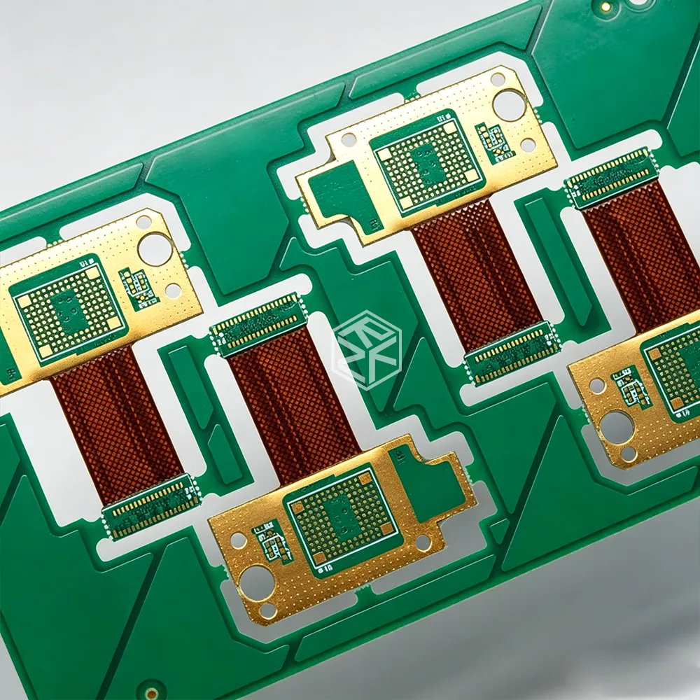
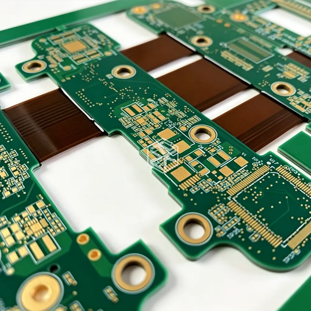
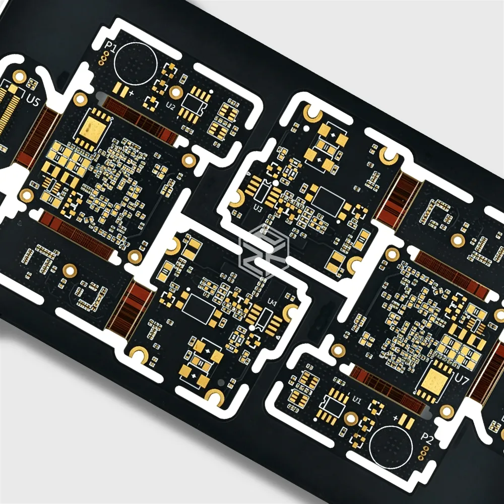
3. Via and Pad Design: Aligning with Process Capability
Via Type and Drill Size
- Through-holes are easiest to fabricate but introduce parasitics
- Blind and buried vias reduce signal distortion but increase cost and complexity
Design Recommendation: Use via types appropriate for your signal bandwidth and tolerance stack-up. Avoid via diameters smaller than 0.2 mm, as they complicate drilling and plating.
Pad Design for Solder Reliability
- Ensure pads match component footprint and reflow profile
- For reflow: optimize pad size for even solder flow
- For wave solder: enable solder drainage with correct pad shape/layout
Avoiding soldering issues: Consider ENIG or selective OSP for high-frequency applications. Avoid oxidized or poorly plated pads which can cause tombstoning, bridging, or cold joints.
4. Common Defects and Engineering Solutions
Line Defects
- Symptoms: Trace opens, shorts, or inconsistent widths
- Causes: Excessively fine lines, poor etch control, misaligned drilling
- Solutions:
- Use conservative etch-friendly geometries
- Monitor etchant chemistry and PCB surface prep
- Calibrate drill machinery and inspect bit wear
Layer Bonding Issues
- Symptoms: Delamination, inner layer shorts
- Causes: Poor lamination pressure/temperature or misalignment
- Solutions:
- Select moisture-resistant prepregs
- Use high-precision lamination alignment systems
- Design with sufficient interlayer clearances
Via and Pad Defects
- Symptoms: Blocked vias, weak plating, pad lifting or oxidation
- Causes: Drill debris, poor plating chemistry, inadequate pad anchoring
- Solutions:
- Enhance cleaning after drilling
- Maintain plating bath chemistry and parameters
- Optimize pad geometry and apply anti-oxidation packaging
Closing the Gap: Manufacturable Design Delivers Value
Companies that embed DFM principles into RF PCB design consistently outperform their competitors:
- Higher first-pass yield
- Fewer reworks or design iterations
- Better long-term reliability
- Reduced customer complaints and warranty costs
In contrast, neglecting manufacturability leads to frequent production delays, lower yields, and unstable product quality—especially in aerospace, medical, or defense electronics, where failure is not an option.
Why Rich Full Joy is Your Ideal RF PCB Partner
At Rich Full Joy, we go beyond design—we engineer for production success. Our experts understand the full lifecycle of high-frequency PCBs, from DFM best practices to advanced RF material processing.
- Precision layout planning for RF applications
- Stackup simulations and impedance modeling
- Design validation with production process alignment
- Yield-optimized designs backed by decades of RF manufacturing experience
Trust Rich Full Joy to help you design performance-driven, cost-effective, and highly manufacturable RF PCBs—engineered from concept to production floor.