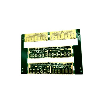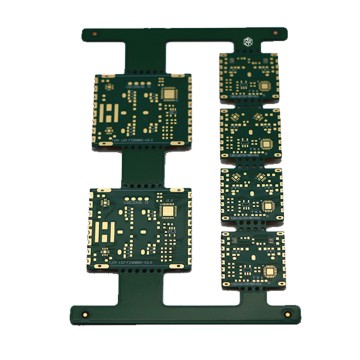
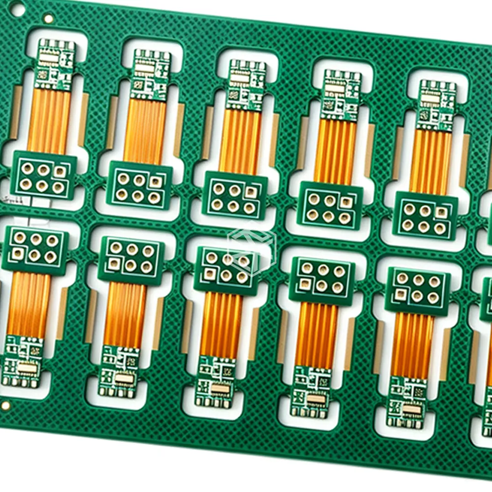
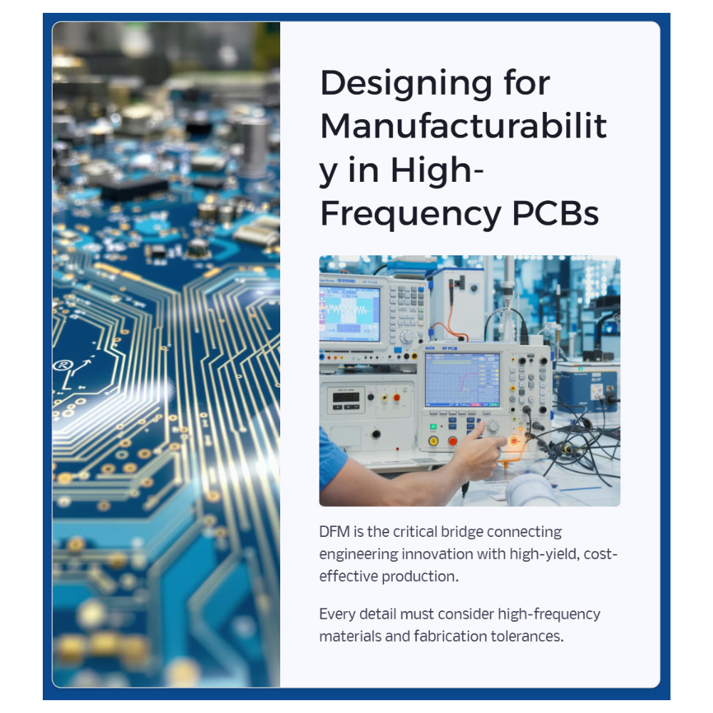
From Design to Performance: How to Prevent Quality Risks in High-Frequency PCB Manufacturing
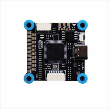
In high-frequency PCB manufacturing, the design phase acts as the cornerstone of quality—just like a foundation determines the strength of a skyscraper. Poor design choices can lead to signal distortion, electromagnetic interference, and manufacturing bottlenecks. For RF PCB design engineers, mastering quality control at the design stage is critical for ensuring performance in applications like 5G base stations, satellite systems, and millimeter-wave communication.
Let’s explore how early-stage design decisions impact impedance control, signal routing, material selection, and structural reliability—while uncovering the root causes of quality issues.
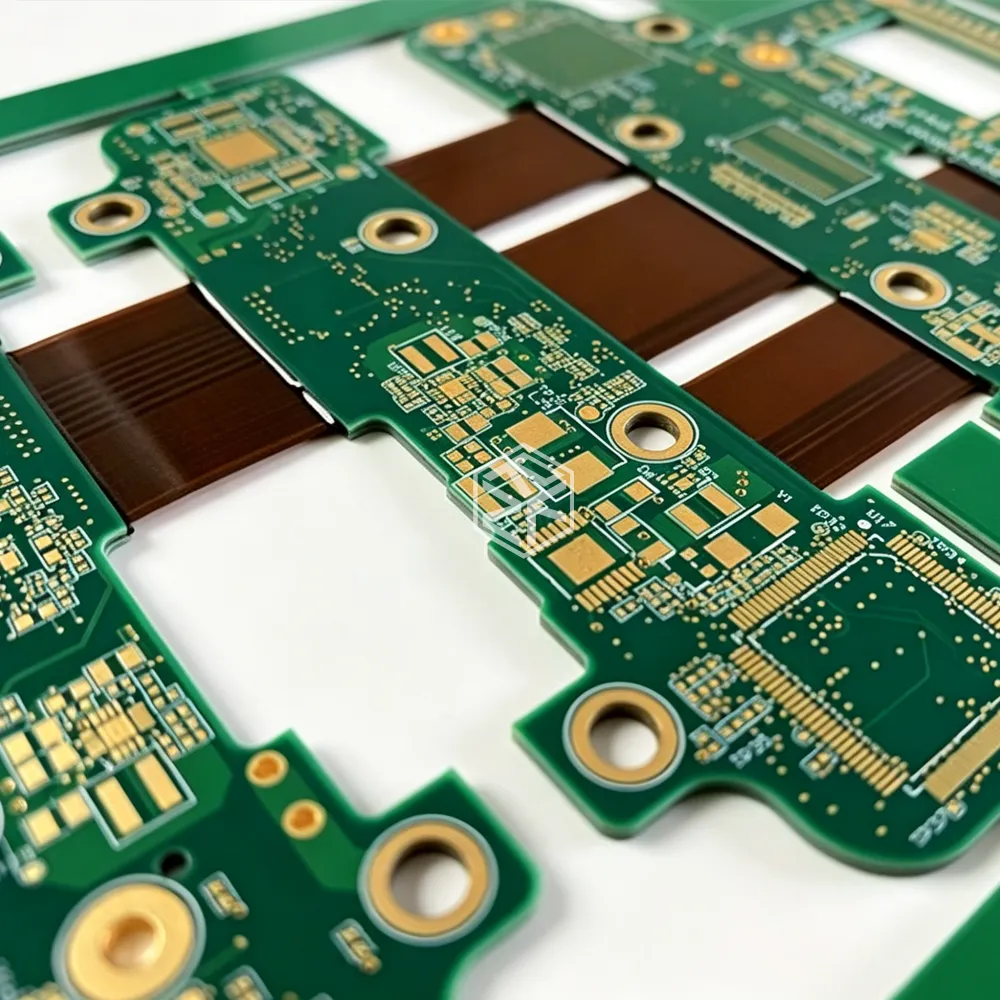
Signal Layer Design: Impedance Matching and Routing Topology
1. Precision Impedance Design1.
In high-frequency circuits, characteristic impedance must tightly match design targets (typically 50Ω or 75Ω, with a tolerance of ±5%) to avoid signal reflection and degradation. Impedance mismatches are like sound waves bouncing off hard walls—reflections distort the signal and lead to increased bit error rates and decreased data throughput.
Achieving impedance consistency requires:
- Accurate trace width and spacing calculations
- Precise dielectric thickness control
- Stable dielectric constant (Dk) materials (e.g., Rogers laminates)
For example, Rogers RO4350B, with a stable Dk and low dissipation factor (Df), is widely used in 5G and mmWave PCBs to ensure low-loss signal transmission.
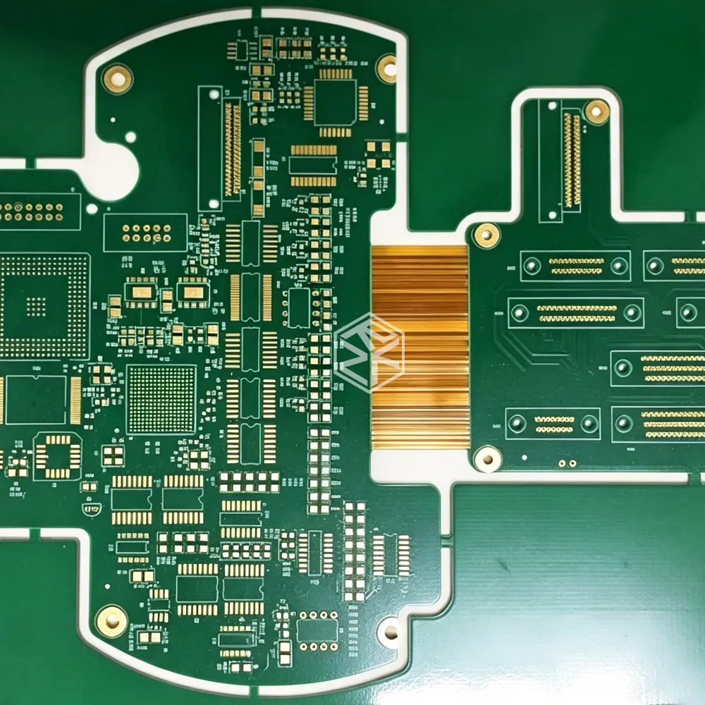
2. Optimized Routing Topology
Trace layout is like urban planning for signal traffic. Poor layout—overly long, narrow, or congested traces—introduce signal loss, delay, or distortion. Dense routing also increases the risk of crosstalk, especially between adjacent high-speed signals.
Industry benchmarks :
- NEXT (Near-End Crosstalk) < -30 dB
- FEXT (Far-End Crosstalk) < -40 dB
To mitigate interference:
- Increase spacing between traces
- Add ground shielding layers
- Use star or daisy-chain topologies based on signal flow
These layout strategies reduce EMI, preserve signal integrity, and improve high-frequency circuit reliability.

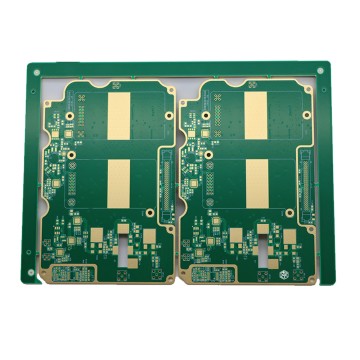
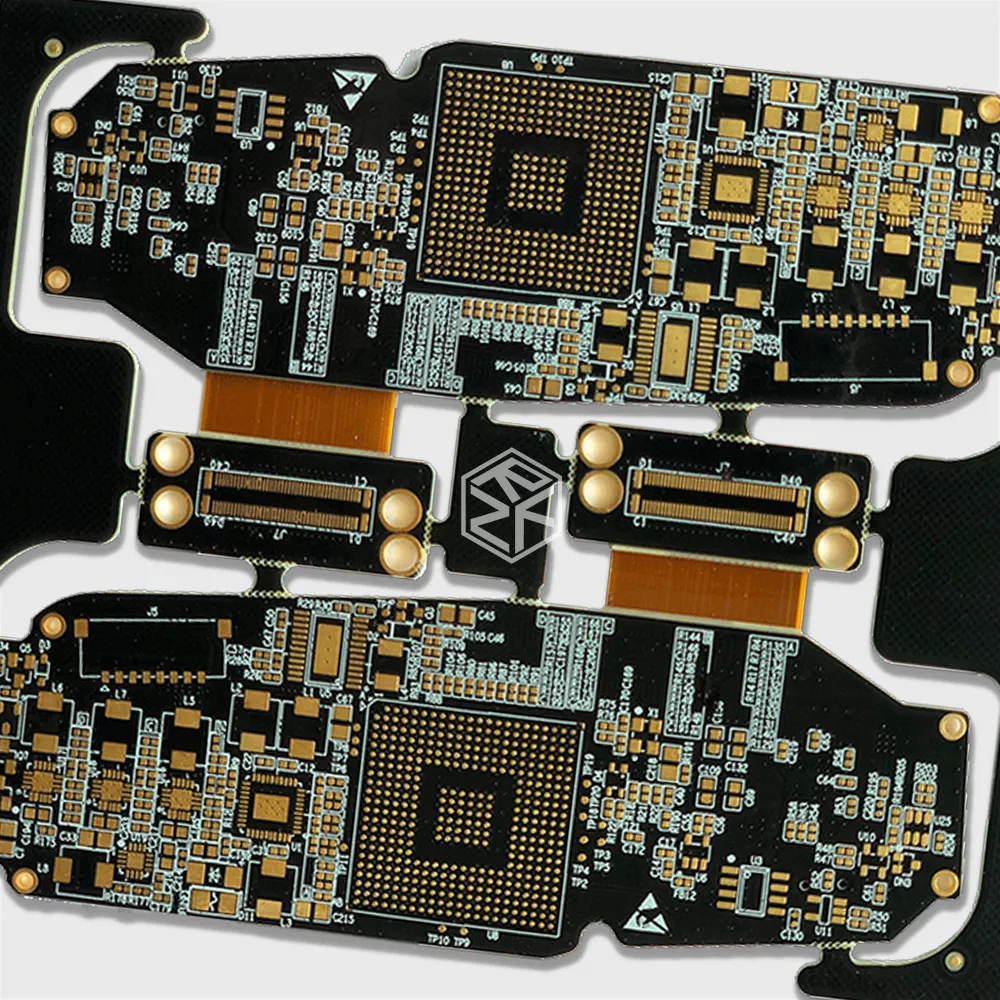
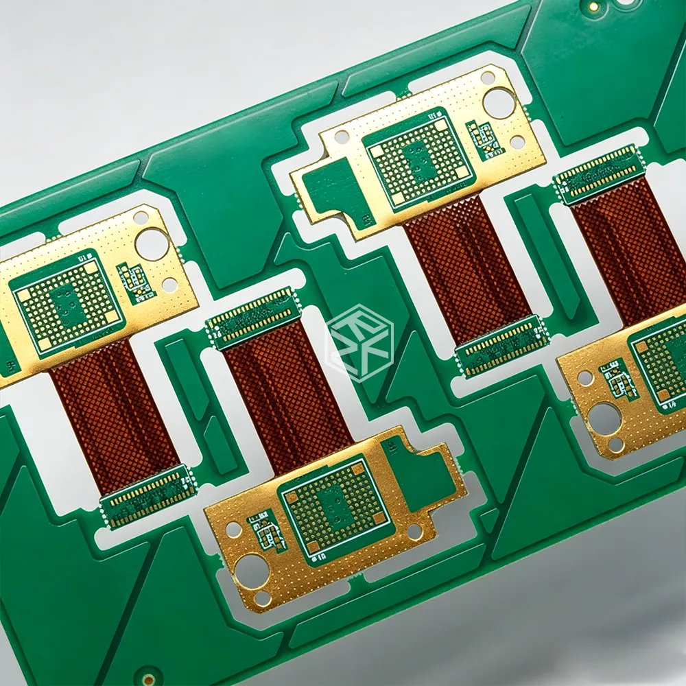
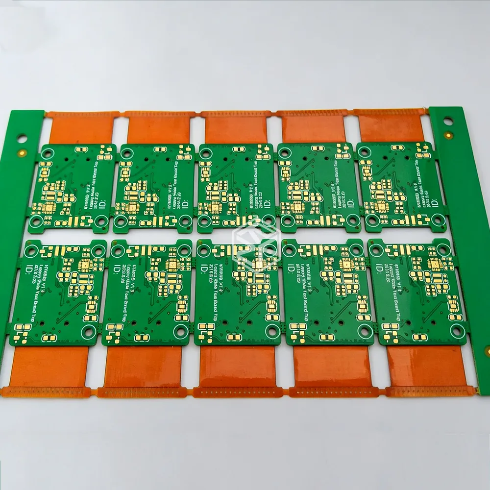
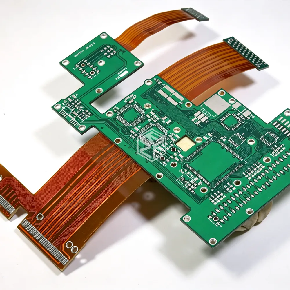
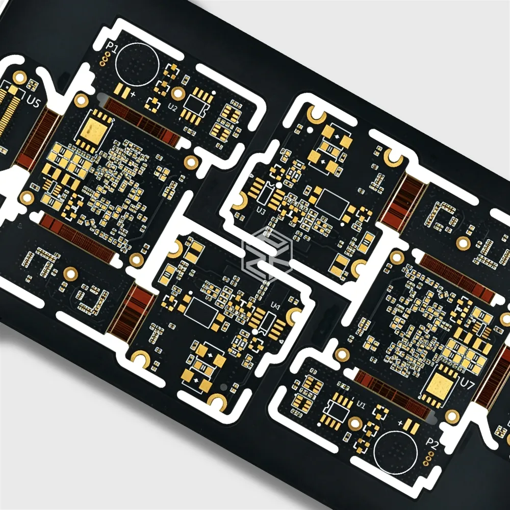
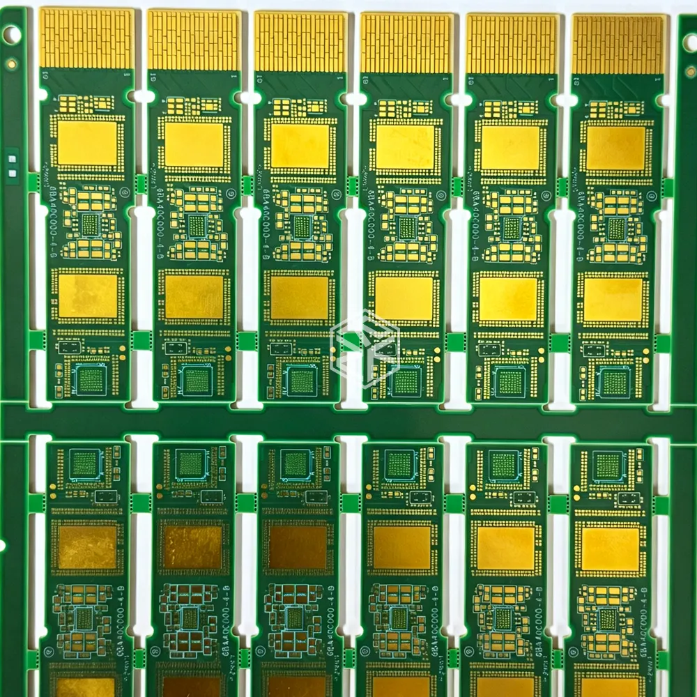
Material Selection & Stack-Up Optimization
1. Substrate Matching for High-Frequency Performance1.
Choosing the right laminate material is critical to managing signal attenuation. For mmWave applications (e.g., 24GHz–52GHz), materials with low Df ensure minimal transmission loss.
Example:
Rogers RO4350B achieves transmission loss as low as 0.5–1 dB per inch, meeting strict mmWave communication standards.
Equally important is Dk stability—fluctuations affect impedance and degrade signal performance. Design engineers must select materials with predictable Dk values under varying temperature and humidity conditions.
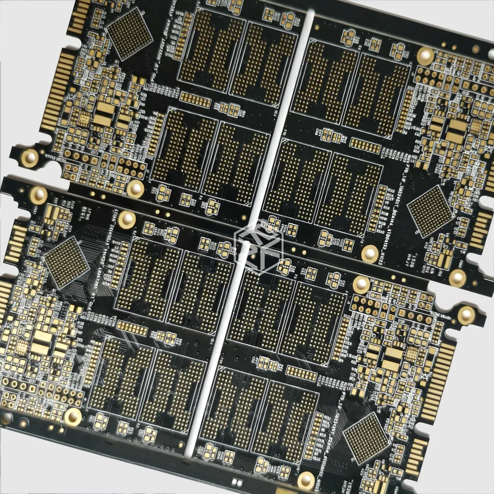
2. Stack-Up Engineering
Layer stack-up influences signal integrity and electromagnetic compatibility (EMC). Well-designed stack-ups can:
- Reduce signal delay
- Minimize crosstalk
- Improve shielding and EMC
Best practices:
- Place power and ground layers adjacent for optimal shielding
- Position signal layers to minimize transmission paths
- Maintain consistent layer spacing for impedance stability
Poor stack-up design—e.g., excessive spacing between signal and ground—can lead to increased delay, radiation noise, and EMI issues.
Common Defects: Causes, Symptoms, and Performance Gap
1. Electrical Performance Issues
Symptoms:
- Signal attenuation
- Waveform distortion on oscilloscopes
- Crosstalk causing data loss or device failure
Root Causes:
- Inaccurate impedance control
- Suboptimal routing
- Inappropriate material selection
- Uneven etching or dielectric thickness
Performance Gap:
Well-designed PCBs show clean, consistent waveforms and high-speed data transfer. Poorly designed ones may cause communication dropouts, network interference, or signal degradation, especially in sensitive applications like 5G base stations.
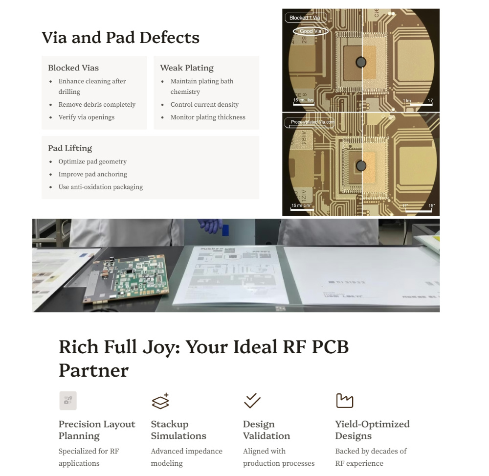
2. Structural Defects
Symptoms:
- Out-of-tolerance board dimensions
- Warping or bowing
- Misaligned or inconsistent hole sizes
Root Causes:
- Incompatible layer thickness design
- Failure to account for mechanical tolerance of manufacturing equipment
- Ignoring thermal expansion and drill wear
Performance Gap:
Reliable boards integrate seamlessly with components and housings. Defective boards increase assembly failures, open circuits, or broken traces, leading to expensive rework and reduced system reliability.
Rich Full Joy: Engineering Quality from Design to FabricationRich Full Joy:
At Rich Full Joy, we believe high-frequency PCB quality starts long before production—with rigorous engineering at the design source. Our team brings:在 Rich Full Joy ,
- Expertise in impedance modeling and stack-up planning
- Knowledge of material characteristics for RF and microwave applications
- Strong collaboration between design and fabrication teams
We help clients eliminate quality risks at the design level, ensuring your products are built for speed, reliability, and global competitiveness.