Achieving Zero-Defect Manufacturing Through Four Technical Pillars
I. Technical Core: Precision Control of Solder Paste Deposition
Industry Insight: “60%-70% soldering defects originate from printing (IPC-7525 7.1.2). Precision deposition is the first line of defense.”
Quantitative Control Targets
| Dimension | Standard Requirements | IPC Reference |
|---|---|---|
| Volume Accuracy | Transfer Rate > 85%, CPK ≥ 1.67 | J-STD-005 4.3.2 |
| Shape Integrity | Slump ≤ 10%, No Tailing/Collapse | IPC-SM-817 3.2.1 |
| Position Accuracy | Offset ≤ 15% of Pad Width | IPC-A-610H 8.2.3.4 |
II. Deep Optimization of Four Technical Pillars
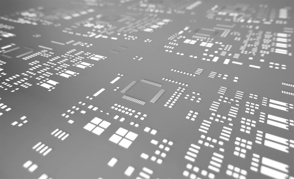
1. Stencil Design: Nano-scale Precision Template
- ·Laser cutting + electropolishing (Ra ≤ 0.6μm, Class 3 compliant)
- ·Step-up/down height ≤ 0.08mm (anti-blade collision design)
- ·SiN nano-coating reduces solder ball defects by 38%
- ·Micro aperture design for 01005 components (area ratio ≥ 0.71)
Design Validation Workflow: PCB → DFM → Prototype → Mass Production
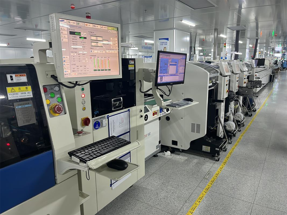
2. Printing Parameters: Closed-loop Smart Control
| Parameter | Standard Range | Risk Threshold |
|---|---|---|
| Squeegee Pressure | 100 ± 20 g/mm | >150 g/mm → stencil deformation |
| Separation Speed | 1.5 ± 0.5 mm/s | >3 mm/s → tombstoning +250% |
| Ambient Conditions | 23 ± 1℃ / 50 ± 5% RH | ΔT > 3℃ → volume fluctuation ±12% |
AI Closed-loop Control: SPI monitoring → LSTM model → dynamic compensation → CPK ≥ 2.0
3. Solder Paste: Full Lifecycle Traceability
- ·Cold storage at -40℃
- ·Stepwise warming: 5℃ every 2h to room temp
- ·Centrifugal mixing: 1200 rpm for 180s
- ·Viscosity check: 850 ± 30 kcps
- ·Open time: ≤ 72h
- ·MES batch binding for traceability
4. Stencil Cleaning: Zero-residue Guarantee
| Cleaning Mode | Frequency | Verification Method |
|---|---|---|
| Dry Wipe + Vacuum | Every 5 PCBs | 50x Microscope Inspection |
| Solvent Deep Clean | Every 30 Minutes | Gravimetric Residue < 0.1 mg |
Scrap Criteria: Tension < 30 N/cm² or >50,000 prints
III. Customer Value: Quantifiable Quality Improvement
| Metric | Before | After | Scenario |
|---|---|---|---|
| First Pass Yield | 82% | 99.1% | 0.4mm pitch QFN |
| Defect Rate | 850 PPM | 62 PPM | Automotive BGA (X-Ray) |
| Rework Cost | $12k/month | $0.8k/month | Medical PCBA Line |
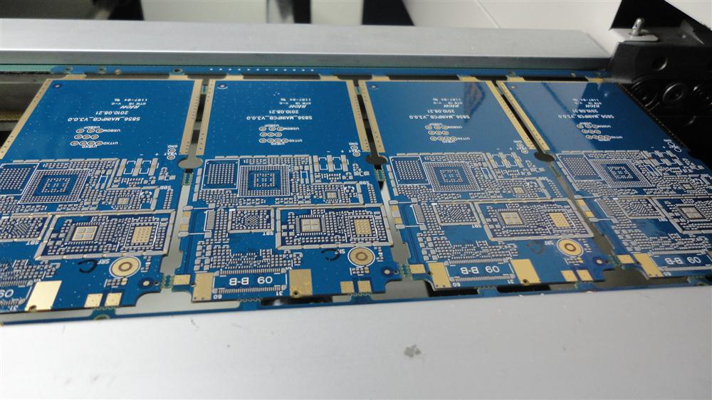
Case: Smartwatch mainboard with 01005 component density achieved zero solder ball defects via nano-coated stencil
IV. Industry Frontier: Era of Smart Printing
Technology Roadmap
- ·2024: Digital twin simulation for stencil printing
- ·2025: Adaptive AI squeegee system
- ·2026: Molecular-level solder paste reactivity control
Professional Insight
"23.7% yield gain achieved by improving paste volume accuracy from ±15% to ±8% (SMTA 2023-PT-087).
Four-pillar technology extends printing defect MTBA (Mean Time Between Defects) to 1200 hours."
References
- 1.IPC-7525C “Stencil Design Guidelines”
- 2.J-STD-005B “Requirements for Soldering Pastes”
- 3.SMTA White Paper: “Solder Paste Deposition Metrics” (2023)
- 4.IEC 61191-3:2017 “Printed Board Assemblies - Part 3”