How a PCB Powers Global Technology? The "Neural Map" Hidden in Electronic Devices
When you scan a QR code for mobile payment, when a car navigation system plots a precise route, or when satellite signals traverse galaxies to reach Earth, an invisible "electronic skeleton" is tirelessly at work—the printed circuit board (PCB). This seemingly ordinary board acts as the neural map of electronics, weaving billions of components into intelligent systems. From roadside shared bikes to deep-sea exploration robots, from chip-level precision substrates to transcontinental communication base stations, over 90% of global electronic devices rely on its support. Today, let’s delve into the world of this "circuit board" to explore how it uses materials and craftsmanship to become the hidden cornerstone of modern technology.

I. Shape-Shifting Magic: From "Electronic Building Blocks" to "Folding Dancers"
1.Layered Labyrinths
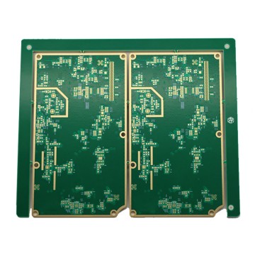
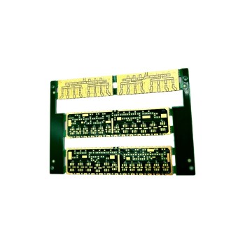
·Simple beginnings: A basic 2-layer PCB functions like a "digital Post-it note," routing connections on both sides. You’ll find these in calculators and remotes.
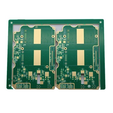
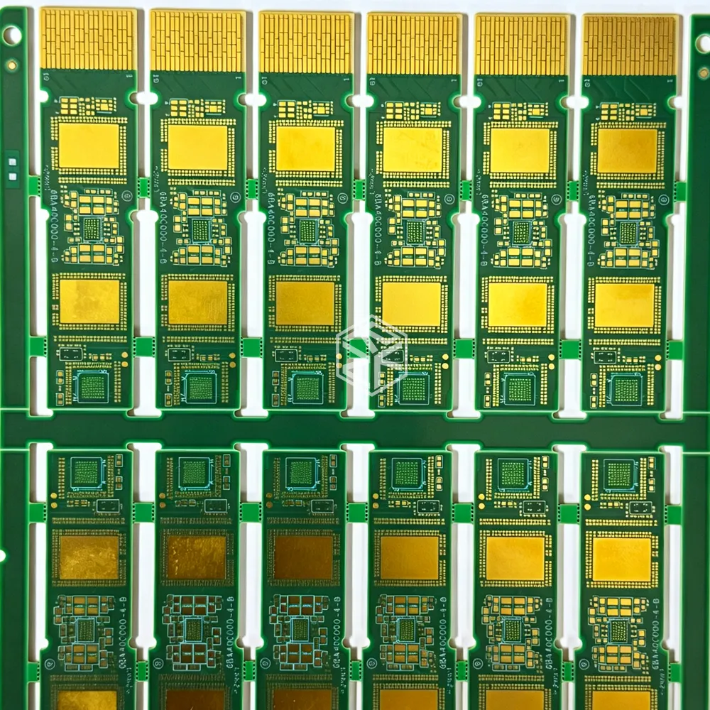
·Complex masterpieces: High-end server PCBs boast 68 layers—a "digital croissant" of precision. These layers (power, signal, ground) fit within a mere millimeter of thickness, akin to stacking 68 ultra-thin sheets of paper in an A4 frame.
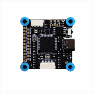
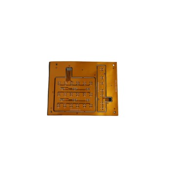
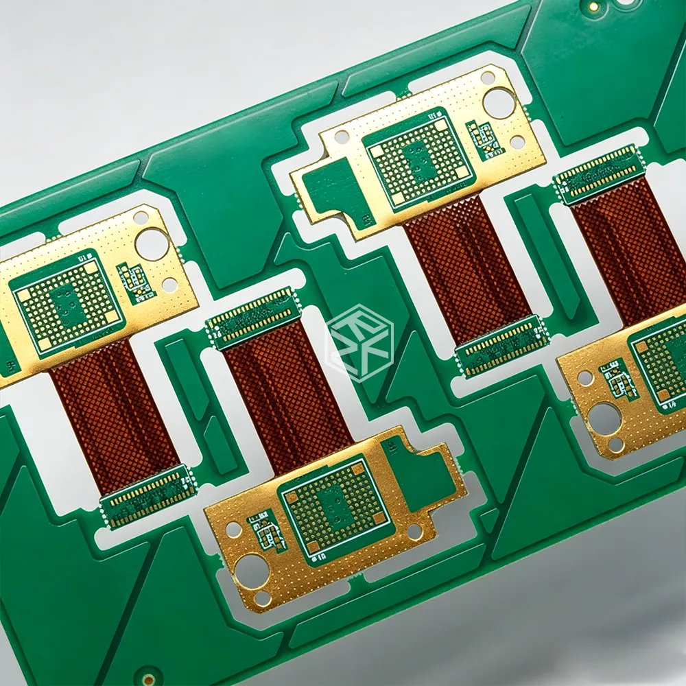
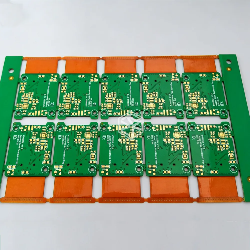
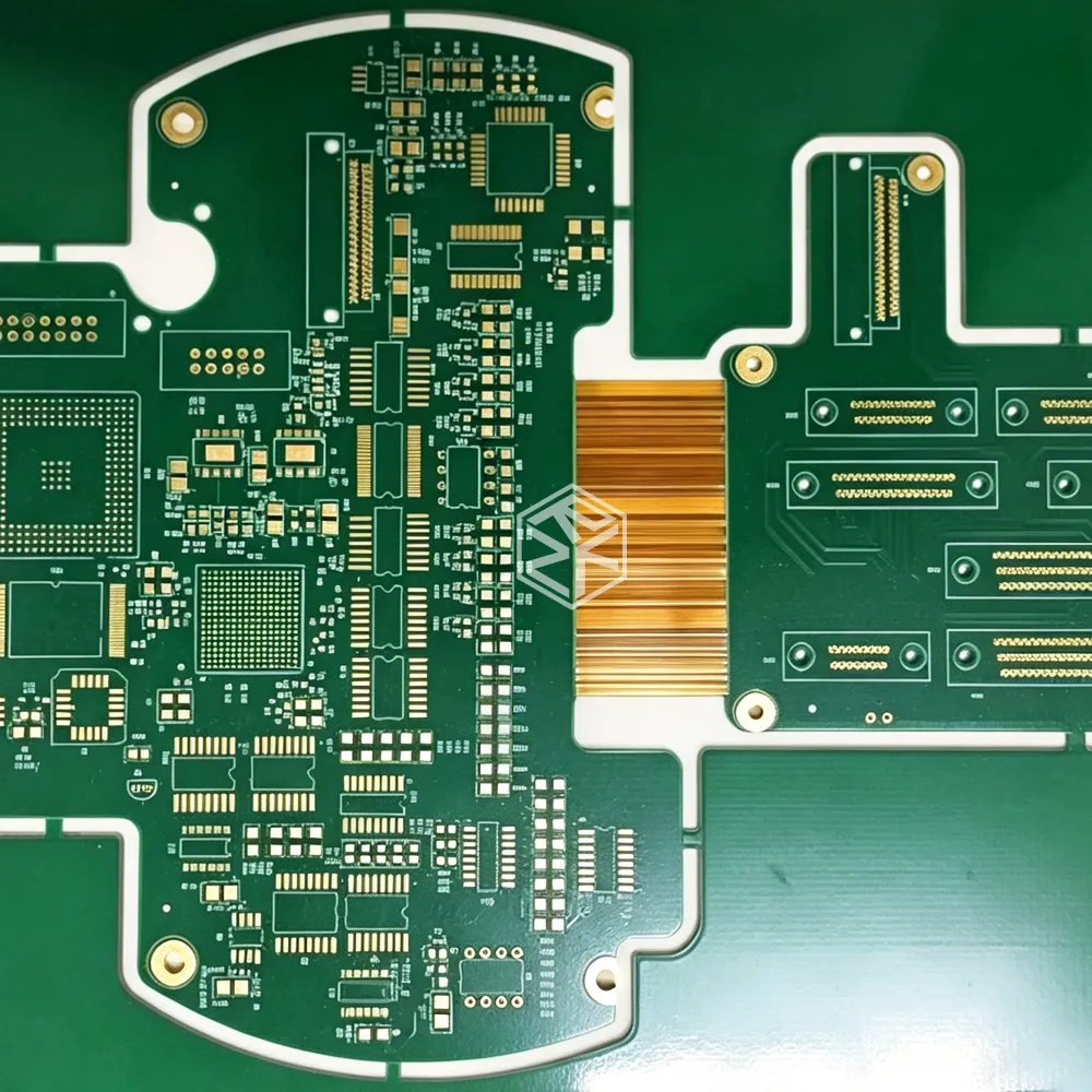
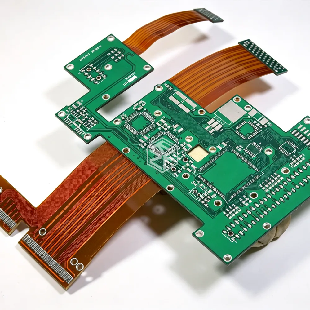
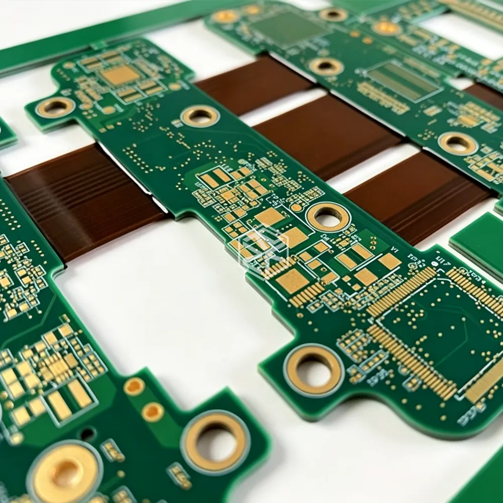
2.Rigid vs. Flexible
·Rigid boards: FR-4 substrates, the "electronic concrete," form the backbone of computer motherboards and TVs.
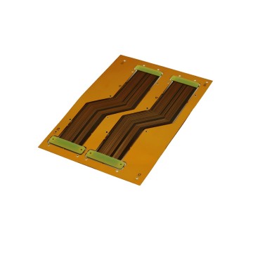
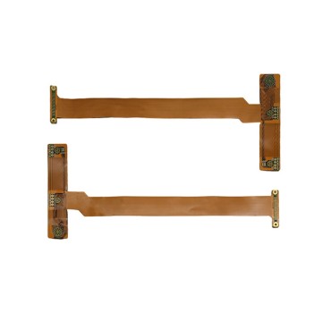
·Flexible marvels: Polyimide (PI)-based flexible PCBs bend 30,000 times without breaking, enabling foldable smartphone screens and heart pacemakers that contour to the human body.
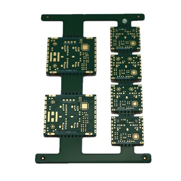
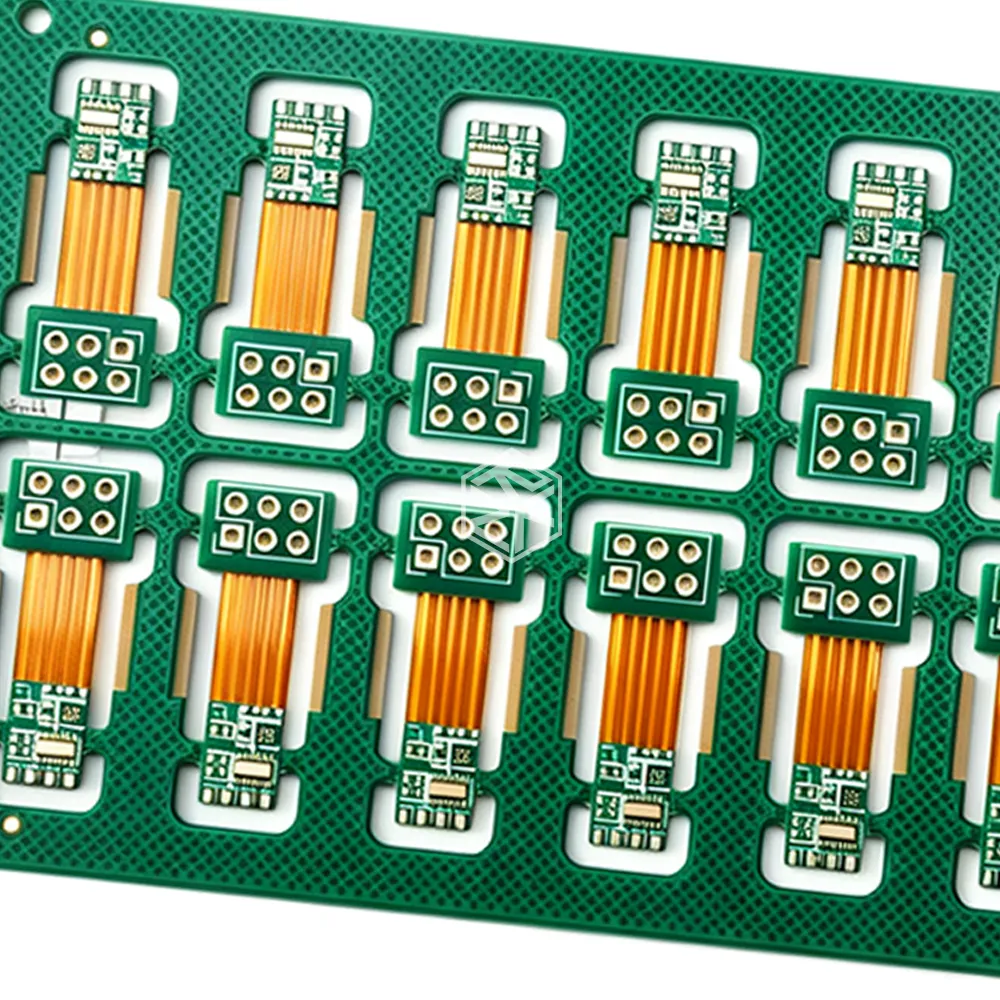
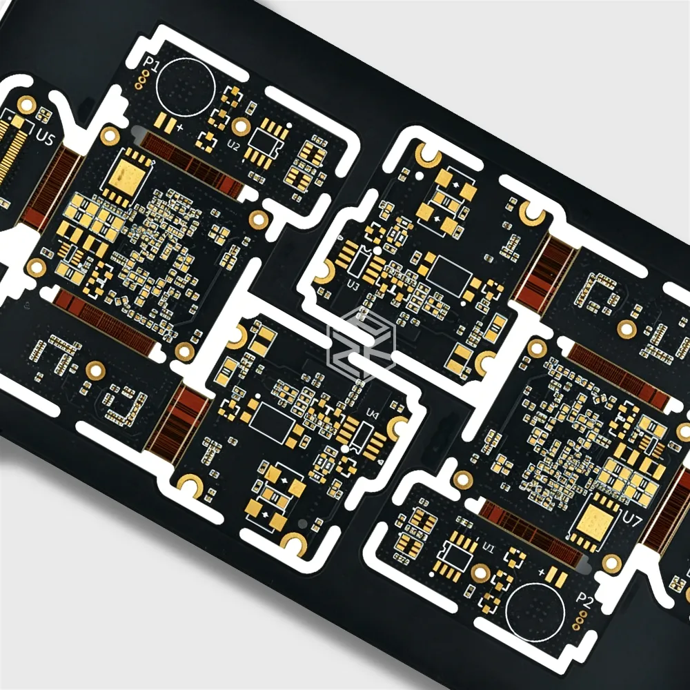
·Hybrid wizards: Rigid-flex designs merge strength and flexibility. For example, earphone internals use rigid segments for chips and flexible sections for cables, balancing function and form.
II. Material Alchemy: From "Thermal Armor" to "Signal Highways"
1.Foundational Protectors
FR-4 dominance: Accounting for 70% of global PCB materials, FR-4 (flame-retardant epoxy) is cheap, versatile, and found in everything from toys to appliances.
Ceramic champions:
- Al₂O₃ substrates: "Heat-resistant armor" for automotive engine modules.
- AlN substrates: With 200x higher thermal conductivity than FR-4, protect 5G base station chips from overheating.
2.High-Frequency Pioneers
PTFE & Rogers: Dubbed "signal superhighways," these low-dielectric-constant materials (as low as 2.1) ensure smooth 5G signal transmission—essential for routers and satellite antennas.
3.Metal Core Innovations
- Aluminum substrates: "Electronic coolants" for LED heat dissipation.
- Thick-copper PCBs: "Power arteries" that carry 100A+, critical for EV battery systems.
III. Nanoscale Craftsmanship: Micron-Level Circuitry
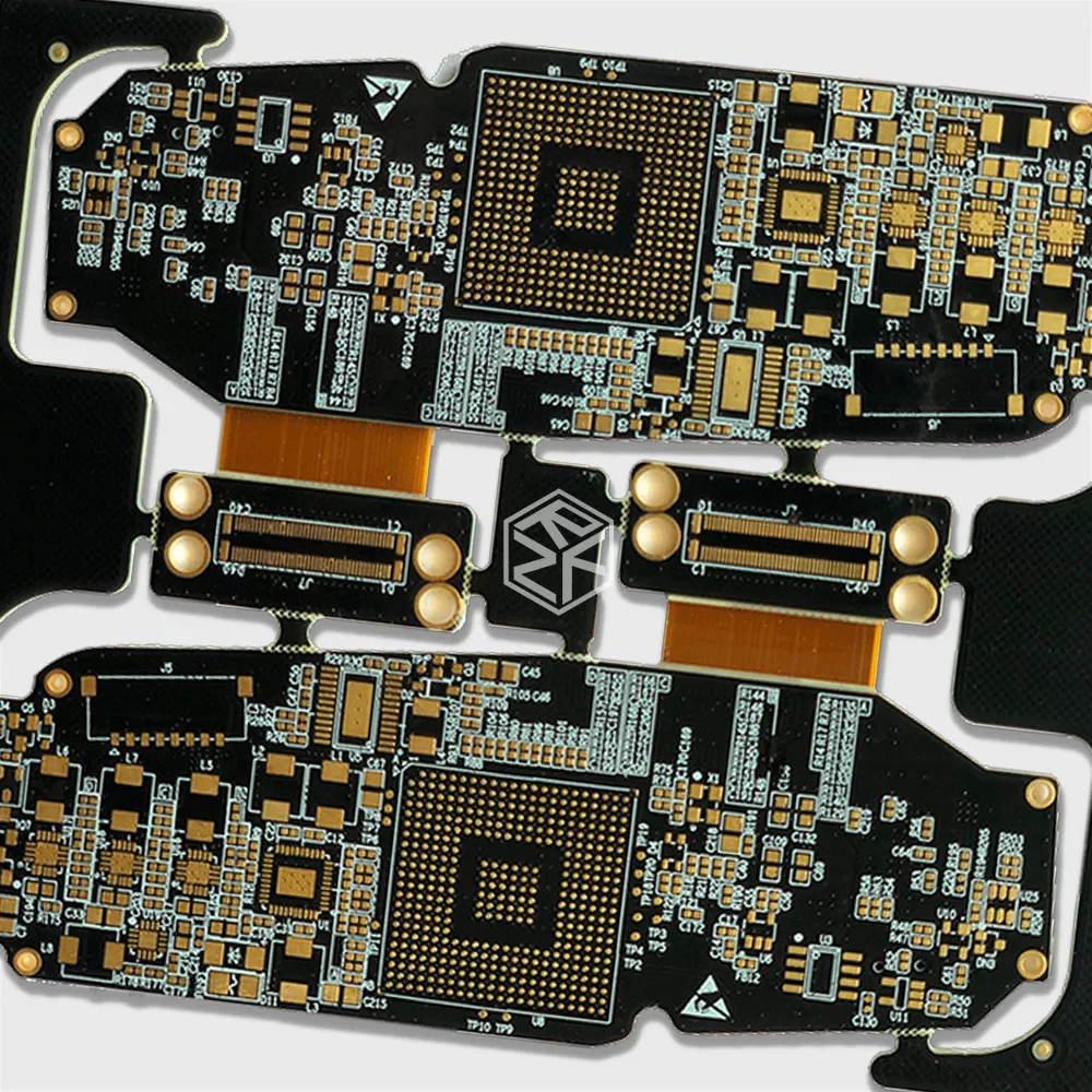
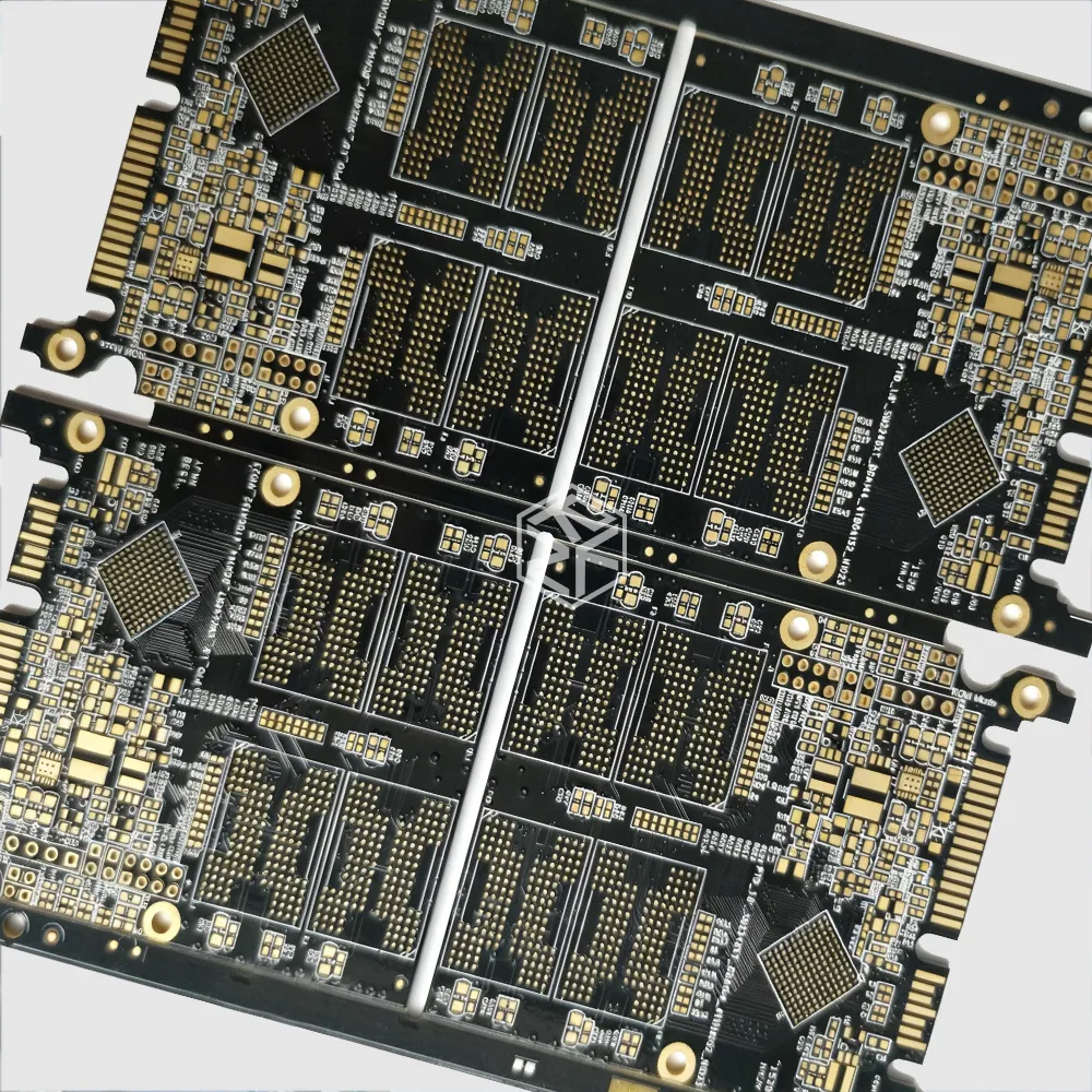
1.High-Density Interconnect (HDI)
Imagine building a city on a fingernail-sized PCB. Microvias (<0.1mm) and blind/buried vias transform flat routes into 3D networks. The iPhone motherboard crams 100,000+ components into 50cm²—equivalent to packing 200,000 people onto an A4 sheet!
2.Surface Finishes: The "Golden Shield"
- ENIG: A nanometer-thin gold layer shields signals from corrosion—ideal for 5G and medical use.
- HASL: Tin-lead coating balances cost and performance for mainstream electronics.
- OSP: A 0.2μm-thin organic film makes soldering easier but needs moisture control.
3.Specialized Techniques
- Controlled-depth drilling: "Electronic acupuncture" that avoids damaging inner layers in critical applications.
- Half-hole PCBs: Allow seamless edge connections to metal casings in industrial equipment.
IV. The Future Unfolds: PCBs in the Age of Intelligence
1.Higher Frequencies
For 6G (100+ GHz), substrates with dielectric constants <2.0 are under development, aiming to halve signal loss.
2.Integration Revolution
Embedded components: Chips and capacitors are buried inside the PCB itself—reducing wearable device volume by 30%.
3.Green Innovation
Lead-free and recyclable substrates (e.g., bio-based epoxy) align with RoHS directives, ushering in a new wave of environmental responsibility in electronics.
Epilogue: Touching the "Neural Endings" of Tech
Next time you dismantle an old phone, observe its corroded PCB. Each winding trace is an engineer’s signature, each tiny solder joint a testament to material ingenuity. Since its invention in 1936, the PCB has evolved from a mere "component carrier" into the metronome of technological progress: flexible boards enabled portability, high-frequency boards built communication bridges, and HDI unlocked limitless chip power.
As we dream of the metaverse, autonomous vehicles, and space exploration, remember—every vision begins with this silent electronic skeleton, carrying trillions of signals across the globe.
The warmth of technology resides in every precise line. Humanity’s future, silently upheld by these invisible "neural maps."