Why Protruding-Type Medical Imaging Probe PCBs Are RF Engineering Platforms
Why Protruding-Type Medical Imaging Probe PCBs Are RF Engineering Platforms
1. From “PCB Design” to “RF Engineering Platform”
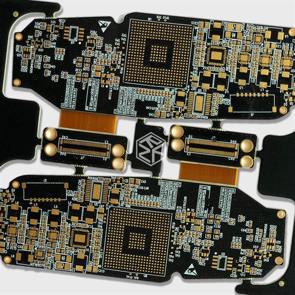
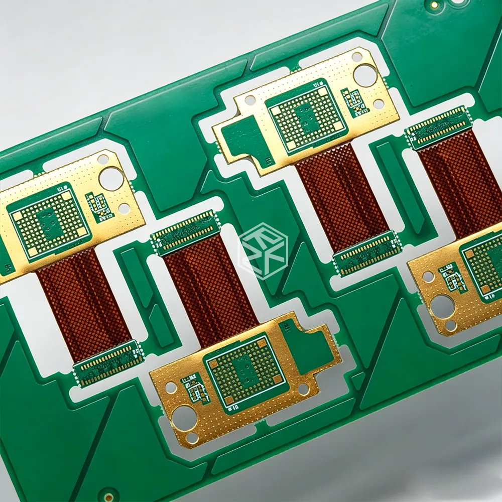
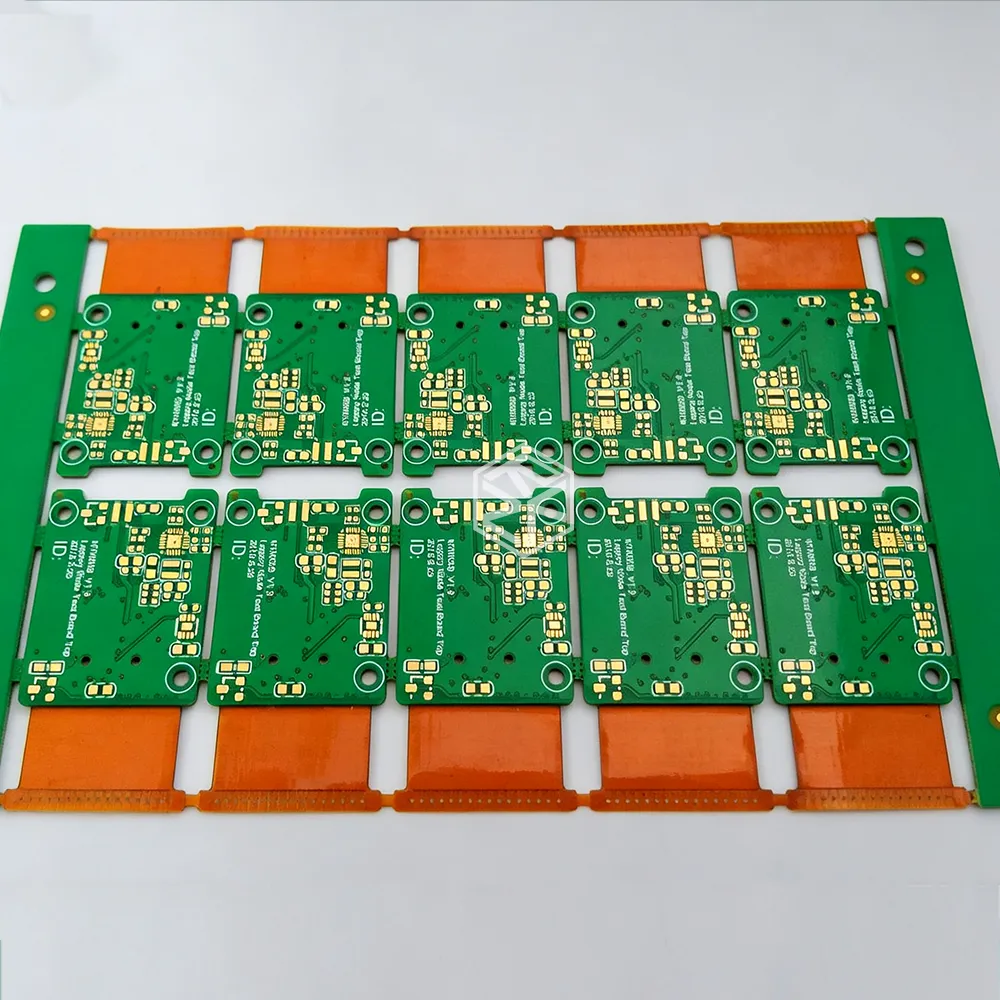
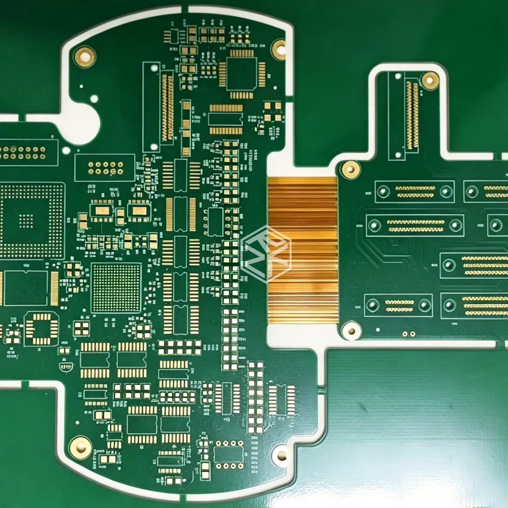
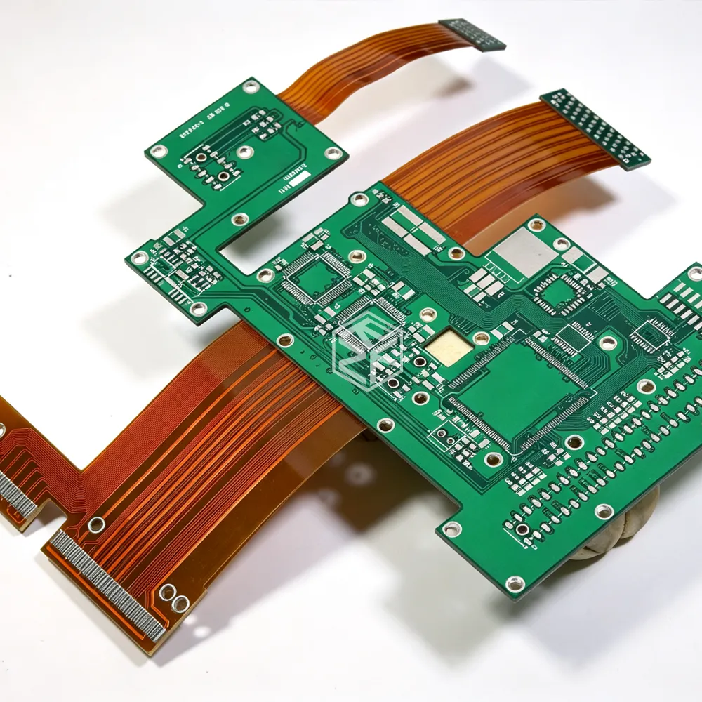
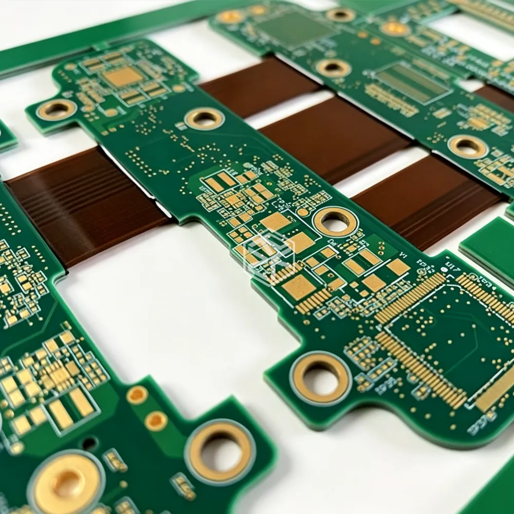
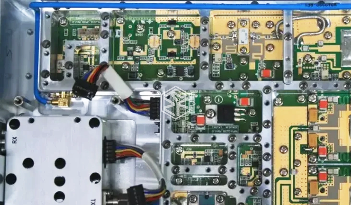
In advanced medical imaging systems, a Protruding-Type Medical Imaging Probe PCB can no longer be viewed as a passive interconnect. It functions as an RF engineering platform, where electromagnetic behavior, structural geometry, and manufacturing precision directly define imaging performance.
Unlike conventional internal PCBs, protruding-type boards extend beyond the device enclosure and operate close to the imaging interface. This exposes them simultaneously to:
- High-frequency RF signal propagation
- External electromagnetic interference (EMI)
- Mechanical stress and micro-deformation
- Extremely low signal-to-noise margins
At this level, the PCB itself becomes part of the RF system—not merely its carrier.
2. Protruding Geometry Fundamentally Changes RF Behavior
The protruding structure is the key reason these PCBs must be treated as RF platforms.
RF Challenges Introduced by Protrusion
- Loss of enclosure-based electromagnetic shielding
- Increased RF radiation and susceptibility
- Edge effects and impedance instability near board boundaries
- Ground reference sensitivity under mechanical stress
Traditional PCB assumptions break down. RF behavior must be engineered in three dimensions, across layers, edges, and transition zones.
3. Why a 10-Layer Architecture Is the Baseline, Not an Upgrade
Medical imaging probes rely on high-frequency, low-amplitude RF signals that are intolerant of noise, coupling, or reference-plane discontinuity.
A 10-layer PCB architecture enables:
- Dedicated RF signal layers
- Multiple continuous RF ground reference planes
- Embedded shielding layers between functional domains
- Independent analog and digital power planes
- Controlled electromagnetic containment depth
Lower-layer-count designs lack sufficient shielding redundancy and reference stability, especially in protruding geometries where external EMI exposure is unavoidable.
4. RF-Centric 10-Layer Stack-Up Logic
A proven RF-oriented stack-up for protruding medical imaging probes typically follows this discipline:
| Layer | RF / System Role |
|---|---|
| L1 | RF Signal (Microstrip) |
| L2 | Primary RF Ground Plane |
| L3 | Shielding Ground |
| L4 | High-Speed Digital / Control |
| L5 | Analog Power Plane |
| L6 | Digital / Isolated Power Plane |
| L7 | Digital Signal |
| L8 | Shielding Ground |
| L9 | Secondary RF Ground Plane |
| L10 | RF Signal / Probe Interface |
This structure embeds RF intent into the PCB:
- RF layers are tightly coupled to solid ground planes
- Shielding layers form electromagnetic cavities
- Digital noise is buried away from RF domains
- Power integrity is preserved without disturbing RF references
The stack-up itself becomes an RF control mechanism.
5. Multilayer Shielding Is a System, Not a Feature
In protruding medical probes, shielding cannot be an afterthought.
Effective multilayer shielding includes:
- Dual-ground-plane confinement of RF signal layers
- Dedicated internal shielding layers
- Dense via-fence structures around RF paths
- Continuous ground stitching across protruding transitions
Together, these elements form a closed electromagnetic environment that suppresses radiation, minimizes coupling, and stabilizes RF performance in real clinical conditions.
6. RF Signal Integrity Under Mechanical Stress
Protruding PCBs experience bending, vibration, and thermal cycling. These factors directly affect RF behavior.
RF-centric mitigation strategies include:
- Transmission-line modeling across protruding zones
- RF trace setback from PCB edges
- Stripline routing for the most sensitive signals
- High-density ground stitching through mechanical transitions
At this level, RF traces are treated as precision transmission lines, not simple conductors.
7. Materials and Process Control Define RF Reality
An RF engineering platform is only as good as its materials and manufacturing discipline.
Key requirements include:
- Low-loss FR-4 or hybrid RF laminates
- Controlled dielectric constant (Dk) and dissipation factor (Df)
- Tight dielectric thickness tolerance
- Medical-grade solder mask with low ionic contamination
- ENIG or hard gold finishes for probe interfaces
Manufacturing must support:
- Precise 10-layer lamination
- Mixed-material stack-up control
- Laser-drilled blind and buried vias
- Controlled-impedance verification
- AOI and X-ray inspection
Minor deviations can translate directly into degraded imaging resolution.
8. Platform Thinking: Where Engineering Capability Matters
Treating protruding medical imaging probe PCBs as RF platforms requires system-level competence, not just fabrication capability.
Rich Full Joy approaches these designs as integrated RF systems by combining:
- Deep understanding of RF propagation in multilayer medical PCBs
- Proven multilayer shielding execution
- Experience maintaining RF integrity across protruding structures
- Verified impedance control and batch-to-batch consistency
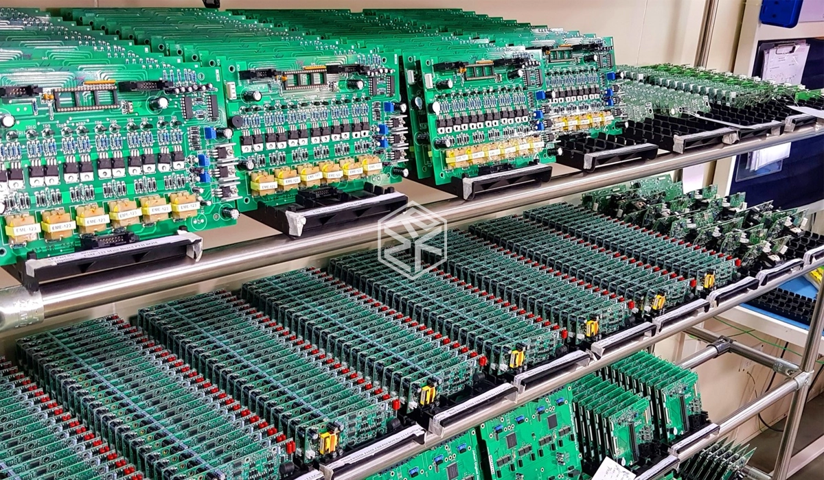
This platform mindset ensures that RF performance is repeatable in production, not just achievable in prototypes.
Core Conclusion
Protruding-Type Medical Imaging Probe PCBs are RF engineering platforms because:
- Their geometry fundamentally alters electromagnetic behavior
- RF performance depends on multilayer architecture and shielding depth
- Mechanical and electromagnetic domains are tightly coupled
- Manufacturing precision directly impacts imaging quality
When designed and built correctly, the PCB becomes a core RF subsystem that enables high-resolution, reliable medical imaging.
This is why protruding-type medical probe PCBs demand RF-first thinking—and why only platform-level engineering can meet their technical threshold.