











Back-Drilled High-Speed Circuit Board for Enhanced Signal Integrity
Why Back-Drilled High-Speed PCBs Are Critical for Signal Integrity
High-speed digital systems are highly sensitive to signal reflections, via stubs, and impedance discontinuities. Back-drilled high-speed PCBs eliminate unused via stubs, reducing reflections and improving signal integrity across high-frequency traces.
A professional high frequency PCB manufacturer ensures:
- Accurate via backdrill depth and precision
- Consistent controlled impedance across the stackup
- Reduced insertion loss for high-speed differential and single-ended traces
- Enhanced electrical performance for multi-GHz interconnects
These engineering measures are essential for server boards, networking hardware, AI accelerators, and high-speed digital applications.
Materials and Stackup Considerations for Back-Drilled PCBs
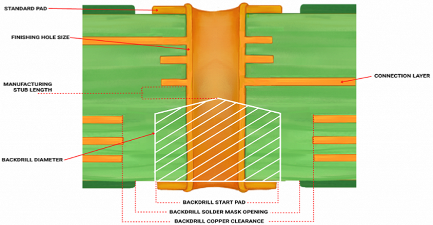
A reliable high-speed PCB manufacturer optimizes:
- Low-loss laminates for high-frequency performance
- Stackups designed for differential pairs, power distribution, and return paths
- Accurate dielectric thickness to maintain target impedance
Engineering considerations include:
- Minimizing signal reflections through precise backdrill execution
- Isolation of high-speed signals from noisy layers
- Optimizing copper thickness and roughness for insertion loss reduction
Proper material selection and stackup planning are critical for maintaining signal integrity in high-density multilayer boards.
Back-Drilling Techniques for Signal Integrity Enhancement
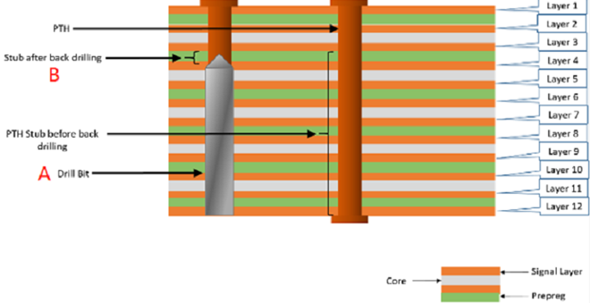
Back-drilling is a precision manufacturing process that removes unused via stubs:
- Laser or mechanical back-drilling removes excess copper
- Improves signal reflection and insertion loss
- Enables tighter differential pair routing in dense HDI layers
A skilled high frequency PCB manufacturer uses:
- Controlled drill depth per layer
- Planarization for uniform surface finish
- Quality verification with X-ray inspection
These practices enhance high-speed signal performance and reduce timing errors in multi-GHz systems.
Controlled Impedance and High-Speed Signal Integrity
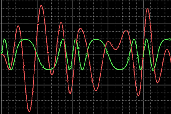
Back-drilled high-speed PCBs maintain precise impedance for high-speed digital circuits:
- Differential pair length matching
- Controlled impedance for high-speed memory and interface traces
- Reduced via stub-induced reflections
Verification techniques include:
- TDR (Time Domain Reflectometry)
- VNA (Vector Network Analyzer) measurements
- Signal integrity simulations
These measures are crucial for AI accelerators, data center server boards, and networking modules.
Thermal Management and Reliability in Back-Drilled PCBs
High-speed digital boards generate significant heat, requiring robust thermal management:
- Copper planes and thermal vias dissipate power efficiently
- Low-CTE laminates minimize warpage
- Thermal cycling testing ensures mechanical and electrical reliability
A professional high-frequency PCB manufacturer ensures back-drilled multilayer boards maintain performance under high-power, high-density conditions.
Manufacturing Process Control for Back-Drilled PCBs
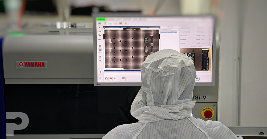
Producing back-drilled PCBs requires precision:
- Accurate layer alignment and lamination
- Controlled via drilling and plating
- AOI, X-ray, and electrical testing
- Functional verification of differential and single-ended signals
An engineering-focused high-speed PCB factory ensures repeatable performance and high yield from prototype to volume production.
Back-Drilled PCBs for High-Speed Systems
Applications include:
- AI accelerator boards
- Data center server motherboards
- High-speed networking switches and routers
- High-bandwidth memory modules
Back-drilled PCBs provide improved signal fidelity, reduced reflection, and higher performance in dense high-speed designs.
Engineering Strength: What Defines a Back-Drilled High-Speed PCB Manufacturer
A top high-frequency PCB manufacturer combines:
- Expertise in back-drill, HDI, and multilayer PCB fabrication
- Controlled impedance and signal integrity verification
- Rigorous QA and electrical testing
- Engineering support for prototyping and high-volume production
This ensures high-speed digital boards meet the demanding performance and reliability requirements of modern computing systems.
FAQ: Back-Drilled High-Speed PCB Manufacturing for Signal Integrity
1. Why back-drill vias in high-speed PCBs? Back-drilling removes unused via stubs, reducing reflections and insertion loss, enhancing signal integrity.
2. What materials are suitable for back-drilled PCBs? Low-loss laminates, hybrid FR-4/high-speed materials, and PTFE-based substrates maintain performance at multi-GHz frequencies.
3. How is impedance controlled in back-drilled PCBs? Precise stackup design, trace width/spacing control, and TDR/VNA verification maintain target impedance.
4. What is HDI technology in PCB assembly? High-Density Interconnect techniques, including microvias and VIPPO, enable compact, high-layer designs.
5. How does back-drilling improve differential pair performance? It eliminates via stubs that cause reflection, improving high-speed differential signaling.
6. How is thermal management handled? Thermal vias and optimized copper planes dissipate heat efficiently for high-speed, high-density boards.
7. What testing validates back-drilled PCB performance? AOI, X-ray, TDR/VNA measurements, and thermal cycling ensure signal integrity and reliability.
8. How many layers are typical for back-drilled PCBs? Multilayer boards often range from 6–20+ layers depending on design complexity.
9. Are embedded passives compatible? Yes, embedded resistors and capacitors can enhance signal quality and reduce footprint.
10. What applications use back-drilled PCBs? AI accelerators, data centers, networking equipment, high-speed memory, and server boards.
11. How does back-drilling affect insertion loss? It reduces stub-related reflections, lowering insertion loss across high-speed traces.
12. What defines a high-quality back-drilled PCB manufacturer? Expertise in back-drill, HDI, controlled impedance, multilayer stackups, and rigorous QA.
13. How is EMI minimized? Optimized stackup, differential pair routing, and embedded decoupling help reduce electromagnetic interference.
14. Can back-drilled PCBs handle multi-GHz signals? Yes, with precise fabrication and controlled impedance, back-drilled PCBs support multi-GHz applications.
15. Why choose a specialized back-drilled PCB manufacturer? Expertise ensures high-speed signal integrity, thermal reliability, and reproducible high-density production.
Conclusion: Partner with a Back-Drilled High-Speed PCB Manufacturer
Back-drilled high-speed PCBs are essential for enhanced signal integrity, low reflection, and high-performance digital systems. From material selection to precise via fabrication and rigorous testing, a specialized high-frequency PCB manufacturer ensures optimal performance in AI, networking, and high-speed computing applications.
Get Expert Back-Drilled PCB Solutions Today
If your project requires:
- AI accelerators and high-speed computing boards
- Multi-layer, high-density PCB designs
- Embedded passives and HDI structures
- Thermal and signal integrity optimization
Connect with a professional back-drilled high-frequency PCB manufacturer
- Free design consultation
- Prototype and sample support
- Stackup and material optimization
- Reliable production at scale
Engineering-grade back-drilled high-speed PCBs









