











Mastering Differential Signal Processing in High-Frequency PCB Design: The Key to Reliable High-Speed Data Transmission
In today’s era of rapid electronic innovation, high-frequency PCBs play a vital role in cutting-edge products. As data transmission rates soar, differential signal processing has become a critical technique for ensuring stable and reliable high-speed data flow. For PCB design engineers, understanding and applying differential signal processing effectively is essential for building top-tier, high-performance high-frequency PCBs.
Fundamentals of Differential Signal Processing
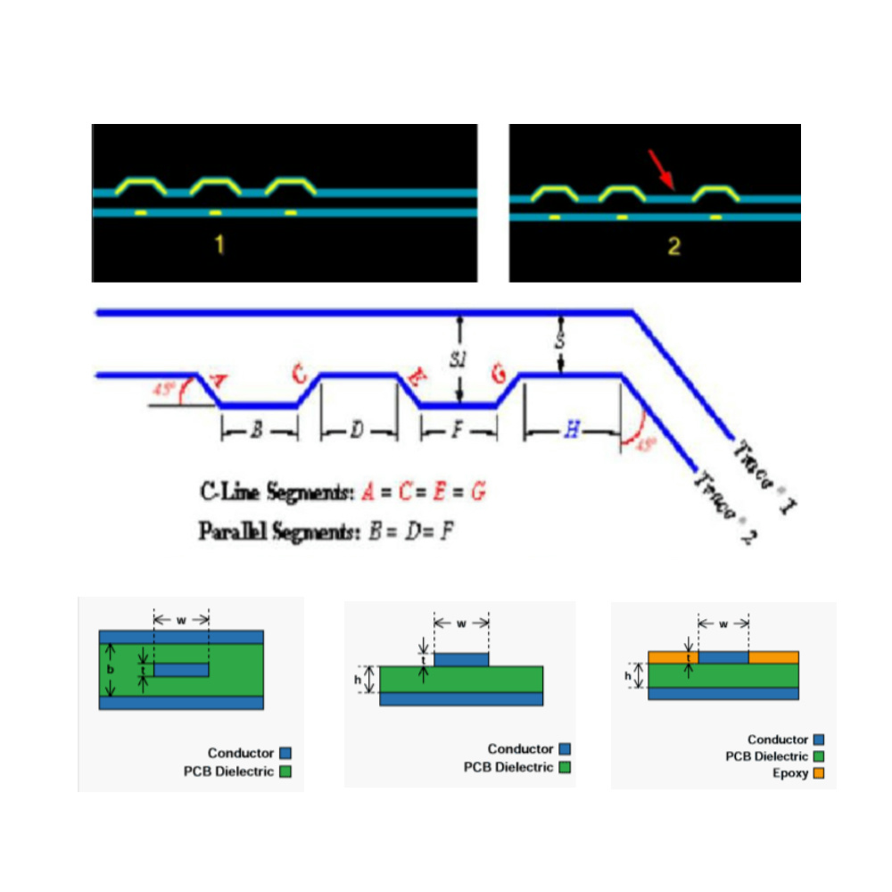
Differential signals consist of two equal but opposite signals transmitted through a pair of lines. Unlike traditional single-ended signals, differential signals are transmitted via differential pairs, offering excellent immunity to common-mode interference.
In high-frequency PCB environments filled with electromagnetic noise, common-mode interference is prevalent. Differential signaling mitigates this by allowing external interference to impact both lines similarly. At the receiving end, a differential amplifier performs subtraction on the signals, effectively cancelling out the common-mode noise and significantly improving transmission integrity. For instance, in 5G communication base stations, which require large volumes of stable high-speed data transmission, differential signal processing effectively combats complex EMI conditions, ensuring accuracy.
Best Practices for Differential Signal Processing in High-Frequency PCB Design
1. PCB Layout and Routing
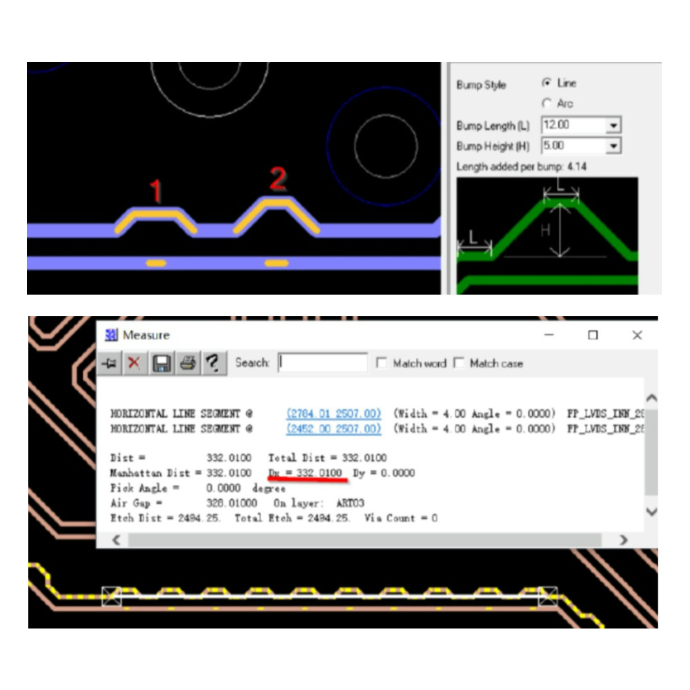
- Length Matching:Keep differential pair lengths as equal as possible. Typical tolerance is within ±5mil. Length mismatch leads to signal skew, affecting timing and signal integrity, increasing jitter and error rates. High-speed serial interfaces like USB 3.0 and HDMI strictly follow this rule.
- Parallel Routing with Consistent Spacing:Differential pairs should be routed parallel with uniform spacing. This ensures consistent mutual inductance and capacitance, minimizing crosstalk and maintaining differential impedance. Typical spacing ranges between 10–20mil, based on dielectric properties and target impedance.
- Avoid Vias and Sharp Corners:Vias introduce parasitic inductance and capacitance, disrupting high-frequency signals. If unavoidable, use appropriately sized vias and consider back drilling to remove excess stubs. Sharp corners should be replaced with 45° or rounded bends to reduce signal reflections.
2. Impedance Matching
- Differential Impedance Design:Differential impedance is a crucial parameter, typically 50Ω, 75Ω, or 100Ω. It depends on the application and interface specifications. Designers must balance trace width, spacing, and substrate Dk values using impedance calculators. A manufacturing tolerance of ±10% is typically acceptable.
- Termination Matching:Proper termination prevents signal reflections. Common techniques include:
- Series Termination:A resistor matching the transmission line’s impedance is placed in series at the source or receiver.
- Parallel Termination:A resistor equal to the differential impedance is placed at the receiver end to absorb reflections. The choice depends on trace length, signal frequency, and driver strength.
Common Defects, Causes, and Solutions
1. Signal Distortion and Bit Errors
- Symptoms:Irregular waveforms, jitter, deformation on oscilloscopes; high bit error rates; data corruption; visual artifacts in video transmission.
- Causes:
- Length mismatch causing phase delay.
- Impedance mismatch leading to signal reflection and distortion.
-
External EMI disrupting clean signal flow.
- Solutions:
- Optimize routing using high-precision EDA tools.
- Strict length matching.
- Improve impedance accuracy using advanced fabrication techniques and impedance testers.
- Apply shielding layers and component placement strategies to mitigate EMI.
2. Crosstalk
- Symptoms:Signal waveforms show noise; amplitude and phase shifts; communication failures.
- Causes:
- Insufficient spacing between differential pairs and nearby signal traces.
-
Inconsistent spacing within the differential pair itself.
- Solutions:
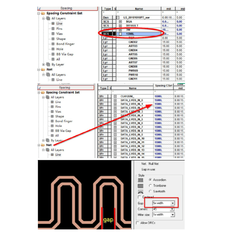
- Maintain spacing at least 3x the trace width between differential and other signals.
- Ensure even spacing and alignment within differential pairs.
- Use ground copper pours around differential lines for shielding.
The Competitive Gap: Precision vs. Deficiency
Enterprises with solid differential signal processing capabilities design high-frequency PCBs that ensure low bit error rates and stable operation in complex environments. These firms dominate sectors like aerospace and HPC by consistently delivering high-quality products, improving production efficiency, and earning market trust.
On the other hand, companies lacking this expertise face challenges such as signal distortion, high defect rates, and customer complaints. This leads to increased after-sales costs, damaged reputation, and loss of market share.
Why Rich Full Joy?
With decades of deep technical expertise, Rich Full Joy excels in RF and high-frequency PCB design—especially in differential signal processing. Our advanced design methodologies, experienced engineering team, and real-world experience enable us to deliver superior, reliable PCBs for high-speed data applications.
We welcome all PCB design engineers to follow our updates. We’ll continue sharing insights into high-frequency PCB innovations as we drive the industry forward together.









