











Failure Analysis in High-Frequency PCB Design: How to Identify and Eliminate Root Causes
In the manufacturing and application of high-frequency printed circuit boards (PCBs), ensuring stable performance and long-term reliability is absolutely critical. When issues like signal distortion, impedance mismatch, or short circuits occur, failure analysis becomes the essential method for uncovering root causes and driving quality improvements.
At Rich Full Joy, with over 20 years of experience in RF PCB fabrication and assembly, our testing engineers rely on precise failure analysis techniques to guarantee product excellence and support rapid innovation. This article outlines the full methodology and practical value of failure analysis in high-frequency PCB development.
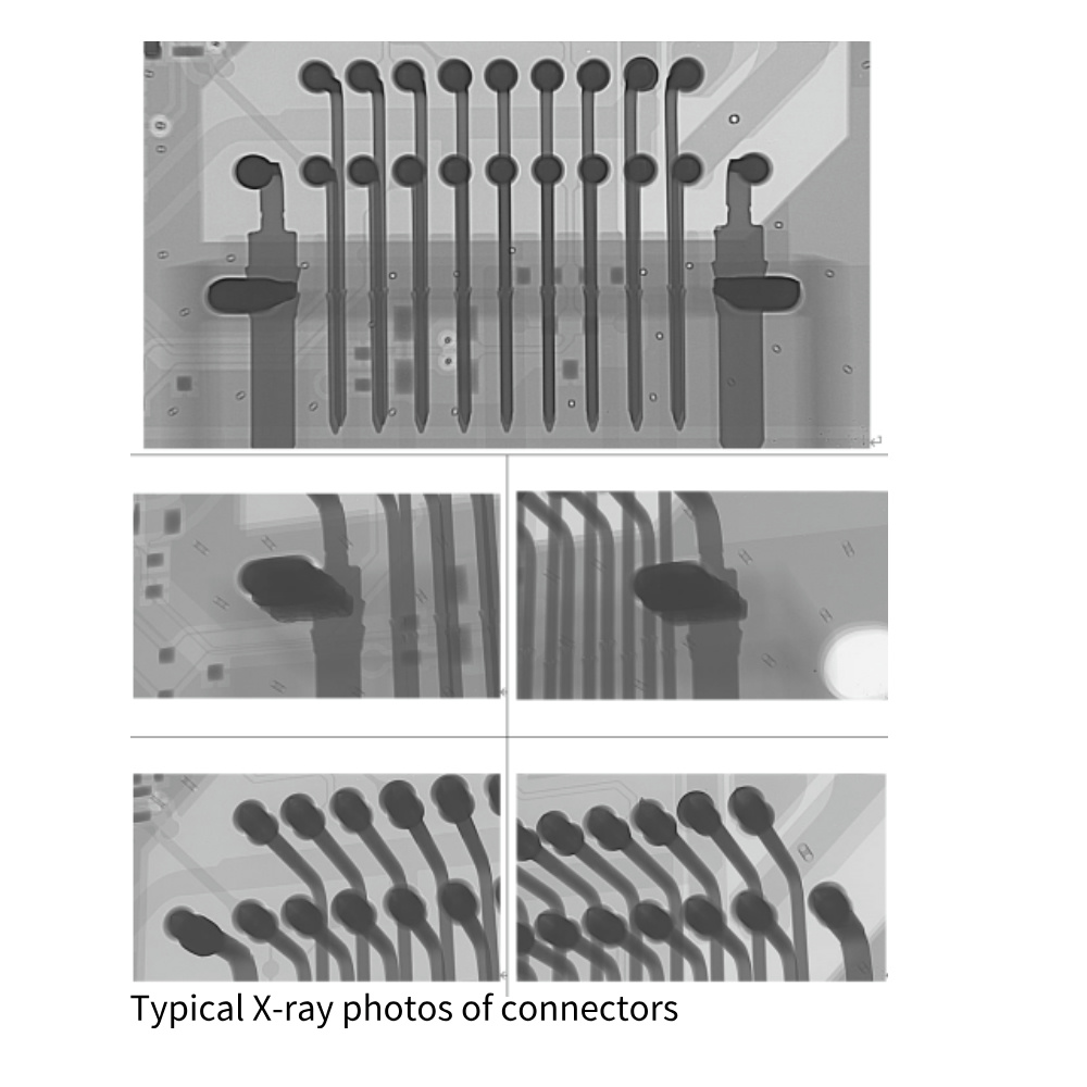
Step-by-Step Failure Analysis Process in High-Frequency PCBs
1、 Failure Symptom Collection and Classification
The first step in failure analysis is a thorough collection and documentation of observed defects during functionality tests, reliability evaluations, or real-world applications. Common high-frequency PCB failure symptoms include:
- Signal attenuation or waveform distortionduring high-speed data transmission tests (e.g., 5G signals)
- Short circuitsfollowing exposure to temperature-humidity reliability testing
- Impedance driftleading to communication errors or system failures
Engineers should record the exact test conditions, time of failure, waveform changes, and circuit response to create a complete failure dataset for root cause tracing.
2、 Visual Inspection
Visual and microscopic inspection is the first non-invasive diagnostic method. Using optical microscopes or magnifying lenses, engineers can spot issues such as:
- Broken tracesor open circuits where copper foil is visibly damaged
- Cold solder jointsor voids, often seen as dull, uneven, or cracked solder connections
- Corrosion marks, discoloration, or scratches caused by chemical exposure or mechanical stress
Example: In corrosive environments, copper traces may darken or thin out due to chemical etching, which could result in intermittent conductivity.
3、 Non-Destructive Electrical Testing
Next, non-destructive testing allows engineers to assess a PCB’s electrical characteristics without damaging it. This includes:
✔️ Impedance Measurement
Using a vector network analyzer (VNA), the characteristic impedance is measured and compared with design targets (commonly 50Ω, 75Ω, or 100Ω). Deviations greater than ±5% often lead to signal reflection, resulting in signal integrity issues.
✔️ Insertion Loss / Signal Loss Measurement
Particularly in millimeter-wave frequencies (e.g., 24GHz–52GHz), insertion loss should remain below 1dB per inch. Excessive loss may indicate poor trace design, improper laminate selection, or internal delamination.
These tests help isolate whether the fault is related to material performance, design inaccuracies, or manufacturing variances.
4、 Destructive Physical Analysis
When surface-level testing doesn’t reveal the issue, engineers move on to destructive methods, such as:
Cross-Sectional Analysis
By slicing the PCB along critical areas, engineers inspect internal layers for:
- Delaminationbetween copper and prepreg
- Layer misalignment
- Internal shorts, voids, or corrosion
Example: If voids appear between bonding layers, it often points to insufficient lamination pressure or uneven heat distribution during pressing.
Scanning Electron Microscopy (SEM)
This advanced technique reveals microstructural defects, such as:
- Hairline cracksin fine-pitch traces
- Micro-voidsin BGA pads
- Contamination residuesnear sensitive analog/RF circuitry
These microscopic evaluations are critical for RF PCB products, where small defects can lead to large performance degradation at high frequencies.
Common Failure Modes, Causes, and Engineering Solutions
Signal Distortion and Bit Errors
Symptoms:
- Irregular waveform shapes
- Jitter or timing errors
- High bit error
Root Causes:
- Differential pair length mismatch, causing skew and phase errors
- Improper impedance matching, leading to reflection and ringing
- External EMIpenetrating unshielded signal lines
✅ Solutions:
- Enforce length matchingwithin ±5 mils
- Design for controlled differential impedanceusing accurate calculators and simulation tools
- Improve shielding, ground isolation, and differential routing parallelism
Crosstalk and Electromagnetic Interference
Symptoms:
- Unstable data transmission
- Intermittent loss of signal or degraded bandwidth
- Unexpected signal coupling between adjacent traces
Root Causes:
- Signal trace spacing too close, especially in high-density layouts
- Non-uniform spacingin differential pairs
- Lack of guard tracesor ground stitching vias
✅ Solutions:
- Enforce 3W rule(trace-to-trace spacing ≥ 3x trace width)
- Optimize pair spacingand symmetry for differential signals
- Apply ground pours, shielding, or via fences to suppress noise
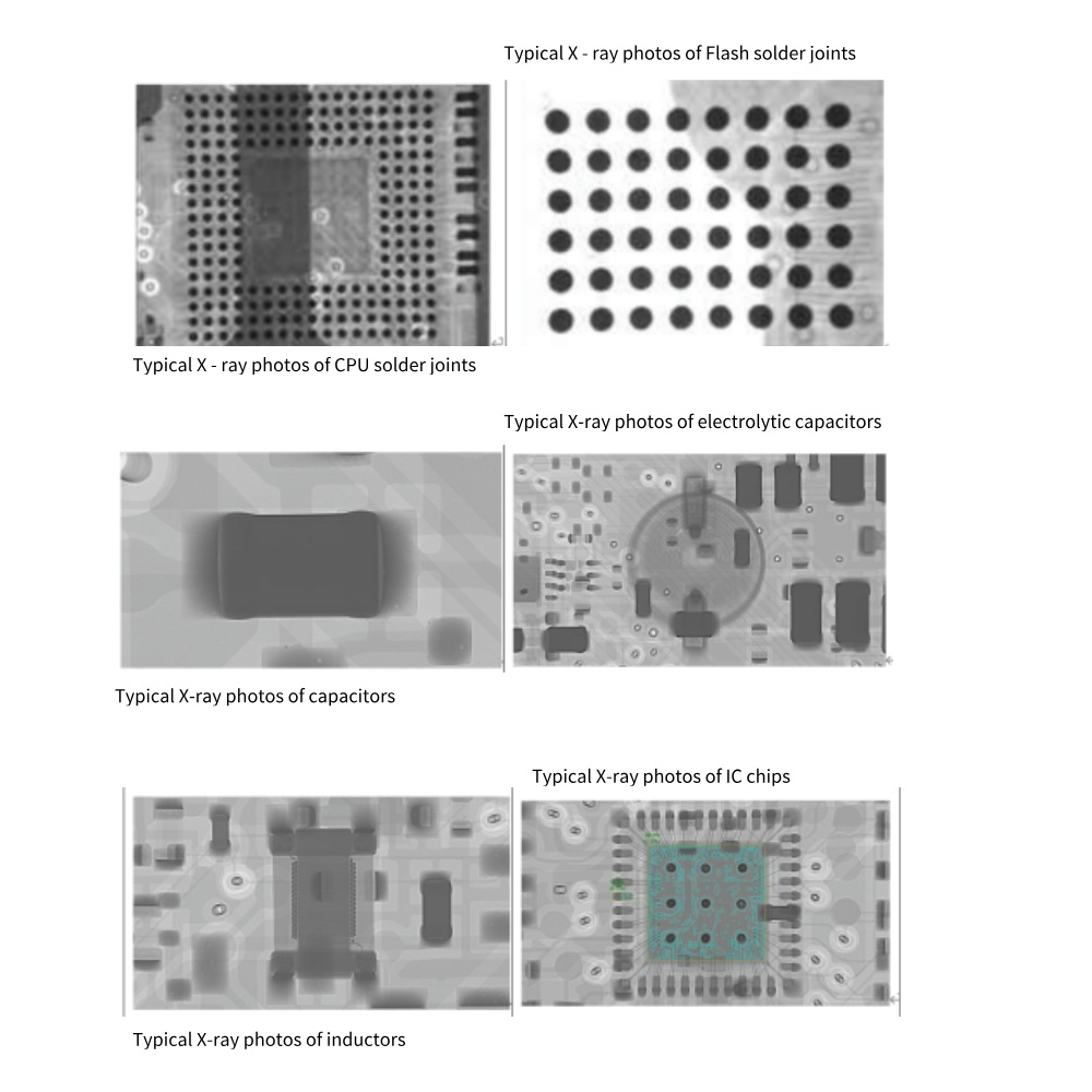
Why Failure Analysis Matters in High-Frequency PCB Development
In high-frequency environments, where data speeds exceed several gigabits per second, the margin for error is incredibly small. Companies that excel in signal integrity analysis and failure detection are able to:
- Maintain ultra-low BERacross high-speed channels
- Achieve first-pass yield improvements
- Reduce costs from rework and warranty claims
- Build customer confidencein product reliability, especially in automotive radar, 5G base stations, and aerospace systems
In contrast, manufacturers lacking robust failure analysis processes often suffer:
- High defect rates
- Frequent returns
- Loss of market trust
Rich Full Joy: Your Partner in High-Frequency PCB Excellence
At Rich Full Joy, we bring decades of expertise to every RF and high-frequency PCB project. From controlled impedance design to comprehensive failure analysis, we support our clients in achieving superior signal performance, even in the most demanding applications.
With our advanced diagnostic tools, skilled engineering team, and precision fabrication standards, we help you identify and eliminate defects—before they become failures.
Contact us today to learn how we can help optimize your high-frequency PCB performance with expert failure analysis and quality improvement support.









