











RF PCB Design from Theory to Practice: A Complete Engineering Guide by Rich Full Joy
In today’s rapidly evolving electronics industry, RF (Radio Frequency) PCB design plays a crucial role in enabling high-speed and high-frequency applications such as 5G communication, IoT, aerospace, and automotive radar. As a company with decades of deep experience in high-frequency PCB engineering, Rich Full Joy is proud to share expert-level insights for PCB designers seeking to master the challenges of RF board design.
RF signals generally operate in the 300MHz to 300GHz range, and designing a PCB for such frequencies introduces unique challenges not seen in low-speed systems. These include signal integrity, EMI suppression, dielectric material performance, and precise impedance matching. In this comprehensive guide, we explore the best practices and design strategies for building reliable and efficient RF PCBs.
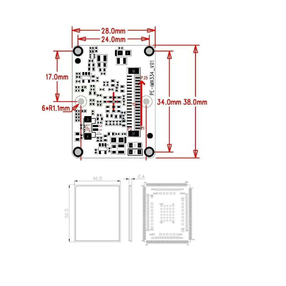
Understanding RF PCBs
An RF PCB is a printed circuit board that operates at radio frequencies, often integrating both digital and analog components, forming what's known as a mixed-signal board. The challenge here lies in managing the interaction between signal types, as improper layout can lead to significant interference and reflection problems.
Depending on power handling, RF PCBs can be classified into:
- Low-power RF PCBs, which prioritize low noise and signal sensitivity
- High-power RF PCBs, which require robust thermal design and power stability
Each category demands unique considerations during the design phase.
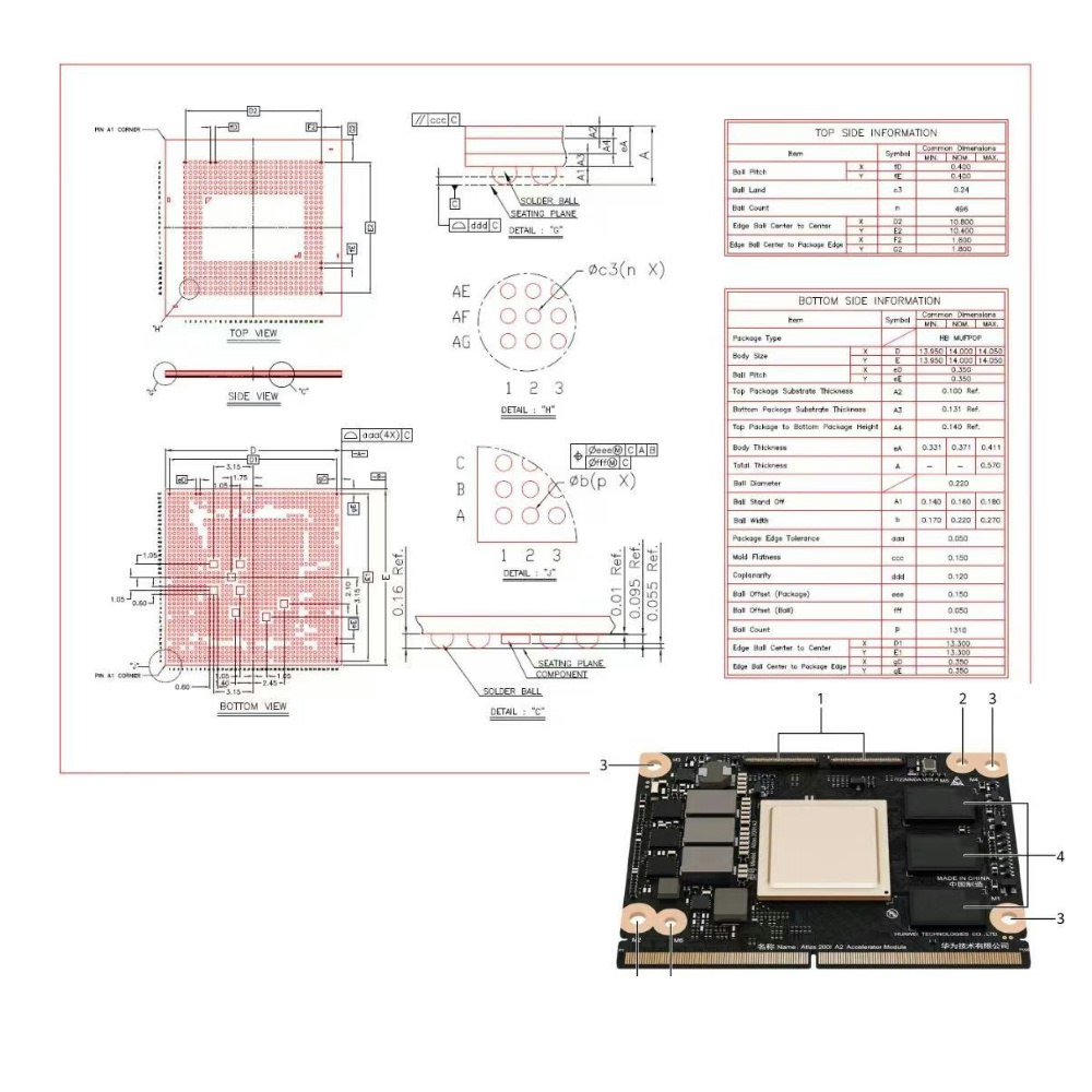
Key RF PCB Design Guidelines
1、 Material Selection: The Foundation of RF Performance
The choice of substrate material directly impacts signal integrity, thermal stability, and impedance consistency across a wide frequency range. Critical parameters include:
Coefficient of Thermal Expansion (CTE)
CTE must be compatible with mounted components. Mismatched expansion rates can lead to cracked solder joints or trace delamination—especially in multilayer RF PCBs. This is vital for high-reliability sectors like aerospace and telecom.
Dielectric Constant (Dk)
Dk defines how quickly signals propagate. RF systems often demand low and stable Dk materials for precise impedance control and reduced reflection. In 5G and millimeter-wave applications, lower Dk materials like RO4350B or RT/duroid are preferred.
Dissipation Factor (Df)
Df indicates dielectric loss. In high-frequency transmission, a low Df is crucial to minimize signal attenuation and maintain clean waveform integrity over distance.
Pro Tip: Materials like RO4000, RO3000, and PTFE-based laminates are industry benchmarks for RF PCBs. Smooth copper foils with low roughness also help reduce signal loss from the skin effect.
2、Optimized Layer Stackup Design
Layer stackup impacts EMI suppression, impedance stability, and signal routing efficiency.
Component Spacing
RF components should be spaced according to their function and power level. Maintain sufficient clearance between high-power devices and sensitive analog circuits to reduce mutual interference and improve thermal dissipation.
Isolated Traces
Avoid floating or isolated traces, which act as uncontrolled antennas. If unavoidable, mitigate them with ground shielding or length control.
Strategic Component Placement
Place components according to signal flow and functional grouping. Shorter interconnects reduce parasitic inductance and signal loss. Allow enough space for test probes and rework access.
Layer Count & Arrangement
Use the top layer for RF routing, ground planes in the middle, and bottom layers for digital or low-speed traces. Balanced stackups with solid ground return paths minimize loop inductance and EMI.
Power Decoupling
Each IC requires localized decoupling to filter power noise. Place decoupling capacitors close to power pins, using proper values for the IC’s frequency and impedance characteristics.
3、Precision RF Signal Routing
RF routing is a science. The goal is to maintain controlled impedance and minimal signal degradation.
Keep Traces Short
Shorter traces equal lower attenuation and reflection. Avoid unnecessary loops in the routing path.
Prevent Parallel Routing
Avoid parallel RF and non-RF traces. Coupled fields lead to crosstalk. If unavoidable, increase spacing and apply ground shielding.
Define Test Points
Test points must be isolated from signal lines to prevent signal distortion during validation.
Smart Bends
RF corners should be rounded or beveled, not sharp. Maintain a bend radius of at least 2x trace width to prevent signal reflection.
Rich Full Joy’s Advantage in RF PCB Design
With over 20 years of engineering experience, Rich Full Joy brings:
- Expertise in RF multilayer board stackups
- Proven impedance controlfor high-frequency performance
- Mastery of low-loss material processing
- Reliable DFM (Design for Manufacturability)reviews to eliminate design flaws early
- Custom support for applications in 5G, radar, satcom, and aerospace
Whether you're building an ultra-compact antenna module or a mission-critical satellite transceiver, we provide tailored RF PCB solutions backed by global industry standards.
Upcoming April Webinars: Unlock Your RF PCB Design Mastery
Ready to go deeper into RF production quality control? Join Rich Full Joy and leading experts this April:
April 14 – 14:00
Multilayer RF PCB Lamination: Key Parameters & Yield Control
- Triple-temperature, triple-pressure lamination model
- Reduce impedance tolerance from ±10% to ±5%
- Boost aerospace RF PCB lamination yield by 32%
April 16 – 16:00
Surface Finish Processes for RF PCBs: Achieve Superior Solderability
- Comparative matrix: ENIG vs. OSP vs. Immersion Silver
- Root cause analysis of mass soldering failures in telecom boards
- Optimized surface finish parameters for high-reliability applications
April 18 – 10:00
Understanding RF PCB Standards: Meeting Industry’s Toughest Specs
- Illustrated breakdown of IPC-2223 high-frequency guidelines
- Size precision control at millimeter-wave levels
- Practical guidance for RoHS 3.1 compliance in RF PCBs
April 21 – 14:00
Controlling RF PCB Quality from the Design Source
- 28-point DFM checklist
- Signal integrity simulation as a pre-production filter
- A case study: Defect-free 5G base station PCB rollout
Join the Movement:
- Follow Rich Full Joy for real-time updates
- Comment your top RF design concern
- Repost & tag 3 engineers to unlock our exclusive RF PCB Quality Control Whitepaper









