











Server Grade High Speed PCB Factory for Cloud Computing Infrastructure
Why Server Grade High Speed PCB Manufacturing Matters for Cloud Infrastructure
In cloud computing infrastructure, processing throughput, network latency, and signal integrity define performance ceilings. A dedicated high speed PCB factory with deep engineering capability ensures that server boards can handle multi GHz signals, PCIe lanes, high speed Ethernet, and dense interconnections without degradation.
A qualified high frequency PCB manufacturer delivers:
• Controlled impedance for high speed traces
• HDI structures for dense routing
• Low jitter and minimal crosstalk
• Thermal reliability under continuous operation
For advanced server and data center applications, manufacturing precision and material control are just as critical as design intent.
High Speed PCB Materials & Stackup Engineering for Server Boards
The backbone of any high frequency circuit board aimed at cloud servers is its stackup and material choice. A true high speed PCB factory optimizes:
• Low dielectric loss materials for high speed signal layers
• Accurate dielectric thickness for controlled impedance
• Layer sequencing to isolate power and clock distribution
Engineering factors include:
• Minimizing skew in differential pairs
• Balancing return current planes
• Ensuring consistent copper distribution across layers
This elevates signal integrity for PCIe Gen4/Gen5, 100/400G Ethernet, and DDR class memory interfaces.
Controlled Impedance & Signal Integrity in High Speed Server PCBs
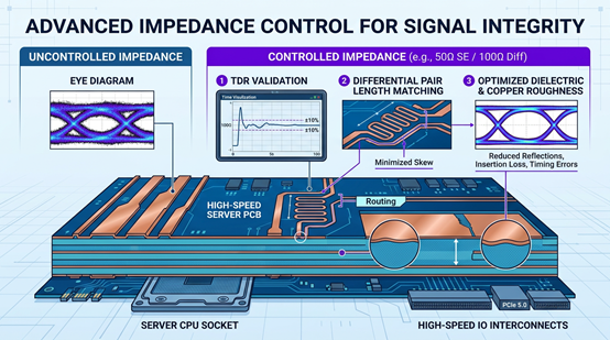
At multi GHz speeds, impedance control becomes paramount. A professional high frequency circuit board manufacturer ensures accurate trace width and spacing, matching target impedances (e.g., 50Ω/100Ω) within tight tolerances.
Key engineering controls include:
• Time Domain Reflectometry (TDR) validation
• Differential pair length matching
• Controlled dielectric and copper roughness parameters
These practices directly reduce reflections, insertion loss, and timing errors—critical for server CPUs, high speed interconnects, and IO buses.
HDI & Microvia Structures for Dense Server PCB Designs
Dense routing and high layer count are typical in server PCBs. A sophisticated high speed PCB factory employs:
• Laser drilled microvias for high pin counts
• VIPPO (via in pad plated over) to improve pad connectivity
• Blind and buried vias to reduce layer transitions
Engineering advantages include:
• Reduced parasitic inductance
• Better signal integrity
• Higher routing density without compromising performance
These technologies expand routing capabilities while maintaining server board reliability.
Thermal Management & Reliability for Server Grade PCBs
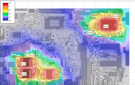
Continuous operation in cloud environments demands robust thermal solutions. A true high speed PCB manufacturer implements:
• Strategic thermal vias for heat dissipation
• Copper pour optimization for power planes
• Material choices resistant to CTE mismatch
• Reliability testing under accelerated conditions
Reliability evaluations include:
• Thermal cycling
• Shock and vibration
• CAF resistance
• Signal integrity over temperature drift
Engineering led thermal control ensures server boards maintain stable performance under load.
Manufacturing Process Control: From Prototype to Volume Server PCB Production
Producing server grade PCBs requires stringent process control:
• Precise lamination of multilayer stackups
• Controlled drilling and plating for vias
• Automated optical and X ray inspection (AOI/X ray)
• Electrical functional testing (Flying Probe / ICT)
A high speed PCB factory with engineering depth ensures repeatability, yield stability, and adherence to complex design rules.
Applications: High Speed PCBs in Cloud Computing Infrastructure
High speed PCB manufacturing enables:
• Server motherboards with high speed I/O
• Network switches and routers
• Storage controllers
• AI & GPU accelerators
Each application requires precise impedance, high layer count, and thermal stability to ensure data center uptime and performance.
Engineering Strength: What Defines a Server Grade High Speed PCB Factory
A leading high frequency PCB manufacturer combines:
• Deep engineering in signal integrity and materials
• Advanced HDI/microvia capability
• Robust quality control systems
• In house engineering support for prototyping and design validation
This blend of engineering and manufacturing excellence ensures server PCBs meet performance, reliability, and scalability needs of modern cloud infrastructure.
FAQ: Server Grade High Speed PCB Manufacturing & Cloud Infrastructure
1. Why choose a high speed PCB factory for server boards?
Server PCBs must handle multi GHz signals with controlled impedance, low loss, and thermal reliability.
2. What materials are best for high speed PCBs?
Low loss laminates with controlled dielectric properties support high speed signals and impedance control.
3. How is impedance controlled in server PCBs?
Through precise stackup design, consistent dielectric thickness, and TDR validation.
4. What is HDI in high speed PCBs?
High Density Interconnect (HDI) uses microvias and advanced routing for compact, high layer boards.
5. Why is thermal management important?
Continuous cloud workloads generate heat; thermal control ensures reliability and signal stability.
6. What testing ensures high speed PCB reliability?
Thermal cycling, CAF resistance, AOI, X ray, and functional electrical testing.
7. Can high speed PCBs support PCIe Gen5?
Yes, with careful impedance control and material selection optimized for high frequency.
8. What role do microvias play?
They reduce signal path length and improve routing for dense server board designs.
9. How many layers do server PCBs typically have?
High speed server boards often range from 8 to 20+ layers depending on complexity.
10. What is controlled impedance tolerance?
Typically ±5% or better for high speed digital signals.
11. Do high speed PCBs require special manufacturing?
Yes — advanced lamination, drilling, plating, and inspection controls are essential.
12. Why is copper roughness controlled?
Copper roughness affects conductor loss at high frequencies and must be managed.
13. What industries use high speed PCBs?
Cloud servers, networking, storage, AI accelerators, and telecom infrastructure.
14. How does signal integrity affect performance?
Poor integrity leads to reflections, jitter, and data errors.
15. How do manufacturers validate high speed PCBs?
Through simulation, measurement (TDR/VNA), and rigorous factory tests.
Partner with a Server Grade High Speed PCB Factory
In modern cloud computing infrastructure, server grade high speed PCBs are critical for performance, reliability, and uptime. From material selection to manufacturing precision and engineering support, every step impacts system behavior.
Get Expert High Speed PCB Solutions for Your Cloud Projects
If your project requires:
✔ Server motherboards and network boards
✔ High speed I/O and data paths
✔ High layer count and HDI routing
✔ Industry grade reliability and repeatability
Connect with a high frequency PCB manufacturer
✔ Free design consultation
✔ Sample and prototyping support
✔ Stackup and material optimization
✔ Reliable volume production capability
Engineered for performance — built for uptime. Contact us today.









