Application of X-Ray Inspection in High-Frequency PCBA Quality Control: How to Identify Internal Defects with Precision
Application of X-Ray Inspection in High-Frequency PCBA Quality Control: Unveiling Internal Defects
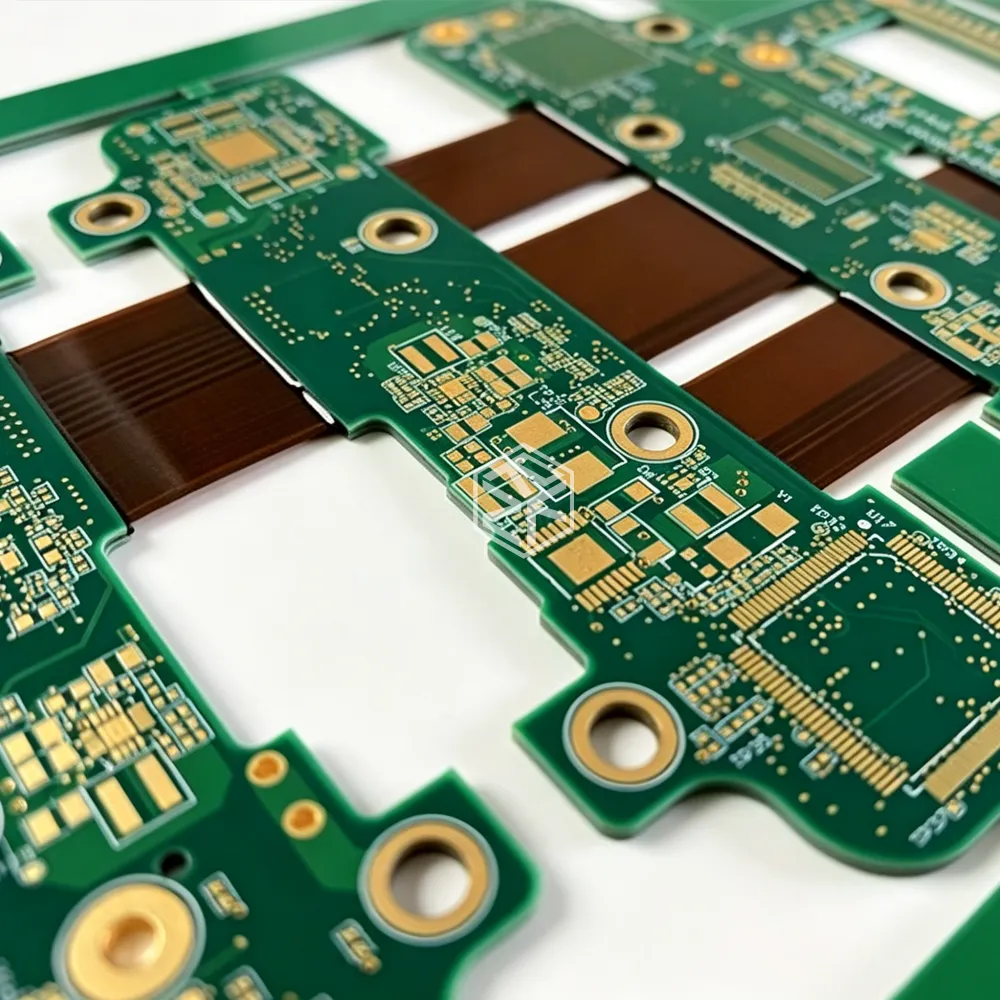
In the realm of high-frequency printed circuit board (PCB) manufacturing, ensuring product quality is paramount. X-ray inspection technology has emerged as an indispensable tool for detecting internal defects that are otherwise invisible, providing a non-destructive means to assess and assure PCBA integrity. For quality control engineers, mastering this technology is crucial to uphold the standards of high-frequency PCBA.
Understanding the Principles of X-Ray Inspection
X-ray inspection operates on the principle of differential absorption, where various materials absorb X-rays to differing degrees based on their density and atomic number. As X-rays penetrate a high-frequency PCBA, components such as copper traces, substrates, solder joints, and internal fillers exhibit unique absorption characteristics. Denser materials like copper absorb more X-rays, appearing darker on the resulting images, while less dense materials appear lighter. By analyzing these contrasts, engineers can identify internal anomalies. For instance, a continuous copper trace should manifest as a consistent dark line; any interruption or irregularity may indicate a defect. This imaging technique offers a clear and effective method for examining the internal structure of PCBA.

Key Considerations for Effective X-Ray Inspection
Optimizing Equipment Parameters
The accuracy of X-ray inspection is heavily influenced by equipment settings, particularly tube voltage and current. For high-frequency PCBA, these parameters should be tailored to the board's thickness and material composition. Inspecting thicker, multilayer PCBA typically necessitates higher tube voltages (ranging from 100 to 160kV) to ensure adequate penetration. Tube current affects X-ray intensity; selecting an appropriate current (commonly between 2 to 5mA) ensures images with sufficient contrast and clarity. Exposure time is another critical factor; both overexposure and underexposure can degrade image quality. Through experimentation and experience, engineers can determine optimal exposure times for various PCBA types, generally spanning from a few seconds to several tens of seconds.
Image Acquisition and Analysis
High-resolution detectors are essential for capturing detailed images of a PCB's internal structures, enabling the detection of minute defects. Modern X-ray inspection systems offer resolutions down to a few microns, revealing intricate details of internal traces. Once images are obtained, specialized software assists engineers in processing and analyzing them. Features such as image enhancement, edge detection, and defect recognition facilitate the identification of issues like trace discontinuities or solder joint anomalies. For example, image enhancement algorithms can improve contrast, making subtle defects more apparent; edge detection techniques delineate the boundaries of traces and solder joints, aiding in the detection of breaks or deformations; and automated defect recognition can highlight areas of concern, streamlining the inspection process.

Identifying Defects: Manifestations, Causes, and the Value of X-Ray Inspection
Internal Trace Defects
1.Manifestations: Internal trace defects can present as breaks, shorts, or corrosion. Breaks appear as interruptions in otherwise continuous lines, shorts as unintended connections between traces, and corrosion as areas where traces have thinned or narrowed.
2.Causes: Trace breaks may result from over-etching during manufacturing or mechanical stress during assembly. Shorts can occur due to incomplete etching, leaving residual conductive material, or misaligned drilling causing unintended connections. Corrosion often stems from exposure to moisture or residual chemicals from the manufacturing process.
3.Value of X-Ray Inspection: X-ray inspection allows for the non-destructive detection of these internal defects, providing clear visualization of trace integrity and enabling timely intervention to prevent potential failures.
Solder Joint Defects
1.Manifestations: Solder joint defects include cold solder joints, voids, and bridging. Cold solder joints may show as incomplete connections, voids as dark spots within the solder, and bridging as unintended links between adjacent joints.Causes: Cold solder joints can arise from insufficient heat during soldering, preventing proper flow and bonding. Voids may be due to trapped gases or contaminants in the solder. Bridging often results from excessive solder application or misalignment during component placement.
2.Value of X-Ray Inspection: X-ray inspection effectively reveals these hidden solder joint issues, facilitating corrective actions to ensure reliable electrical connections and overall PCB performance.
Interlayer Defects
1.Manifestations: Interlayer defects, such as delamination or voids between layers, appear as separations or air pockets within the PCB structure.
2.Causes: These defects can occur due to inadequate lamination pressure, temperature inconsistencies during manufacturing, or contamination between layers.
3.Value of X-Ray Inspection: By detecting interlayer anomalies, X-ray inspection aids in identifying and addressing issues that could compromise the mechanical strength and electrical performance of high-frequency PCB.
Comparative Analysis
Companies that implement advanced X-ray inspection techniques can efficiently and accurately detect internal defects in high-frequency PCBs, leading to a significant increase in first-pass yield rates. Early detection and resolution of defects result in products that exhibit stable performance and low failure rates, reducing costs associated with post-sale repairs and enhancing market competitiveness. Conversely, companies lacking adequate X-ray inspection capabilities may overlook internal defects, leading to inconsistent product quality, increased returns, and reputational damage, highlighting the critical importance of this technology in maintaining industry leadership.
Rich Full Joy possesses extensive expertise in the RF PCB sector, with a profound understanding of high-frequency PCB characteristics. Our proficiency in applying X-ray inspection technology enables us to deliver precise and efficient quality control services for high-frequency PCBA. We warmly invite quality control engineers to engage with us as we continue to share cutting-edge insights into high-frequency PCBA quality assurance, contributing to the ongoing advancement of industry standards.