
PCB Knowledge
Ultimate Guide to Next Generation High Frequency PCB Materials (PTFE / Low Dk Resins)
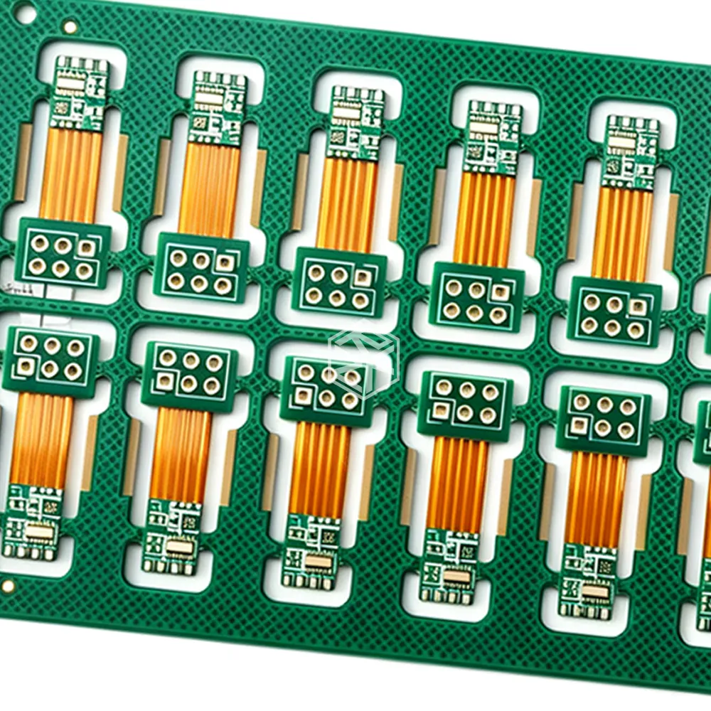
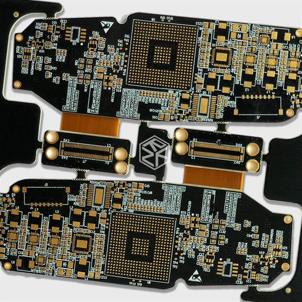
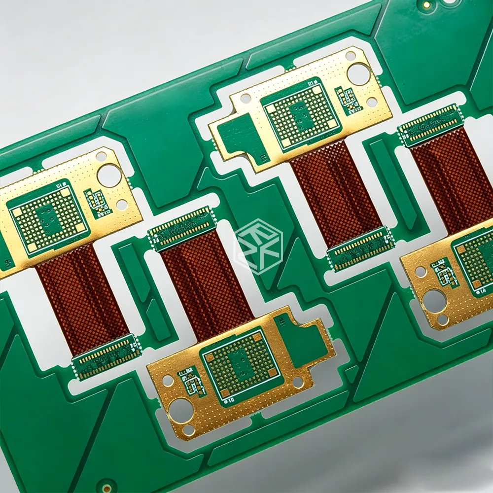
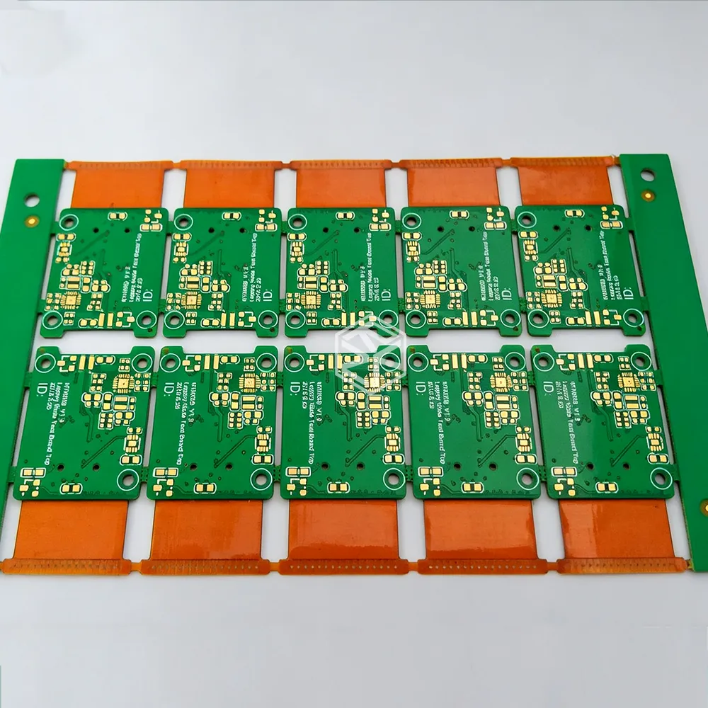
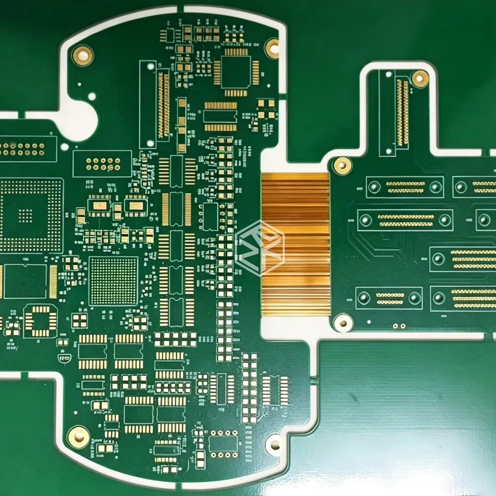
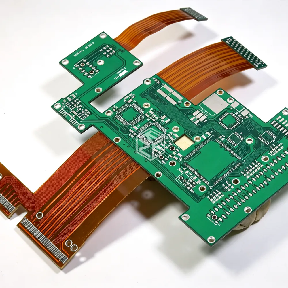
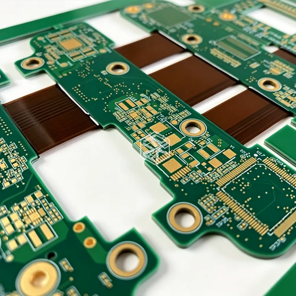
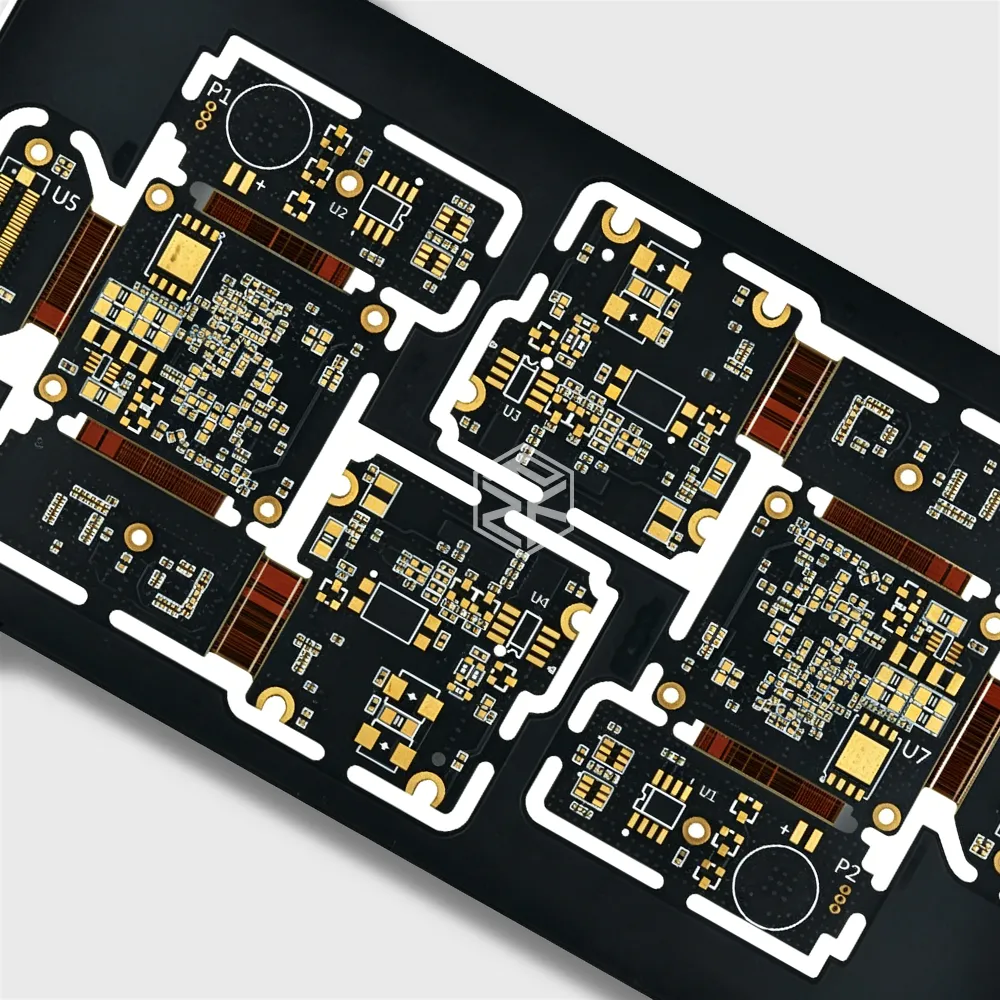
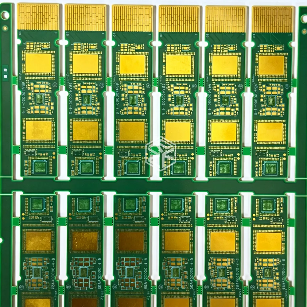
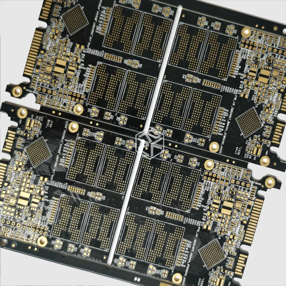
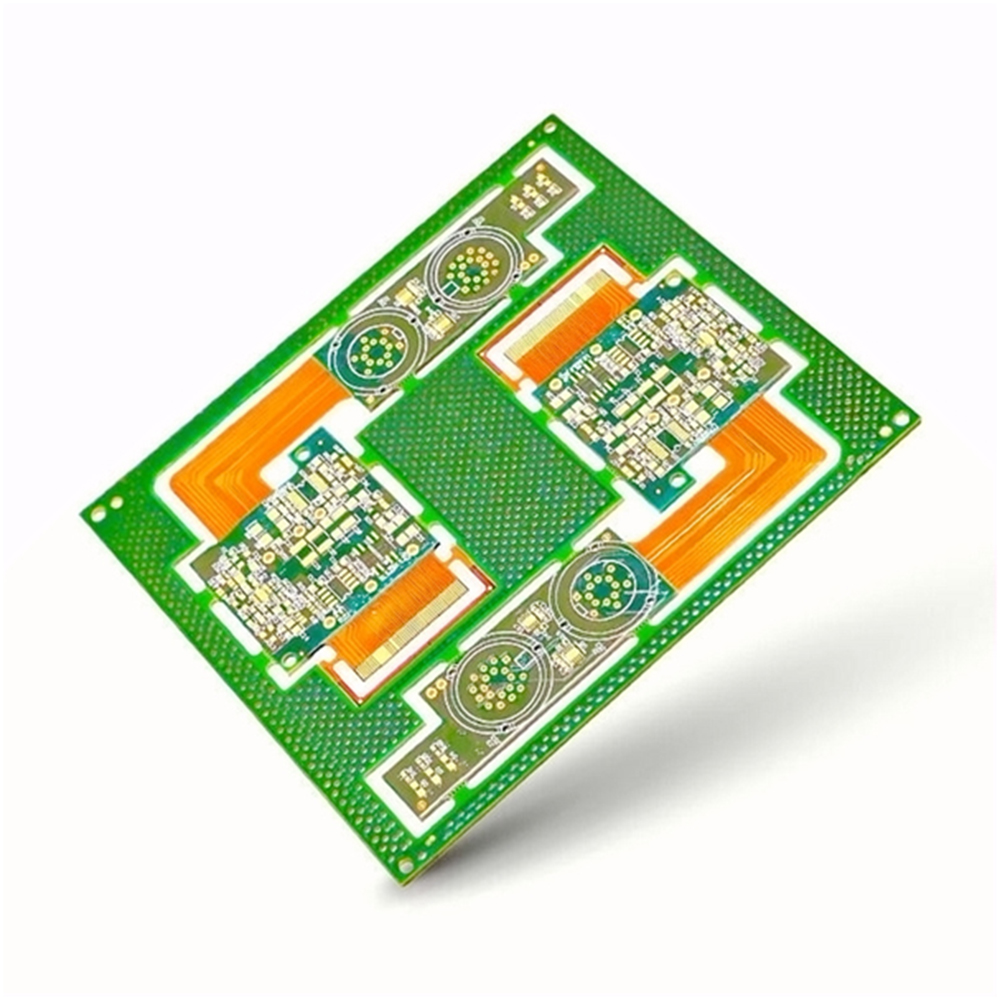
Exploring the Future of HDI: When System-in-Package (SiP) Meets mSAP and Advanced HDI Substrates
We deliver advanced HDI substrate solutions integrating System-in-Package (SiP) and mSAP technology to achieve ultra-fine routing, microvia interconnects, and high-speed signal performance. Designed for next-generation electronics, our solutions bridge the gap between semiconductor packaging and PCB manufacturing.
Boosting HDI Capability: From Design to Production — Integrating Technology, Application, and Reliability
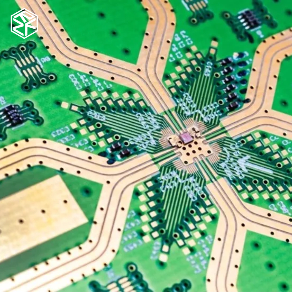
We are a Tier 1 HDI PCB manufacturer in China specializing in mSAP technology, ultra-small vias, and high-density interconnect solutions. Our capabilities support fine-pitch BGA, RF systems, IoT devices, and automotive-grade electronics with full traceability and IPC Class 3 compliance.
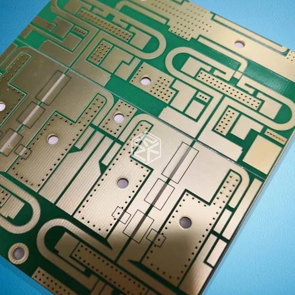
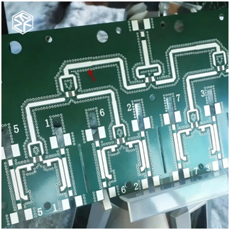
Protruding-Type 10-Layer Medical Imaging Probe PCB — An RF-Centric Engineering Platform
Why Do Long-Stored PCBs Short at Open Vias?
Can Long-Stored PCBs Still Be Used? Technical Guidance & Reliability Analysis
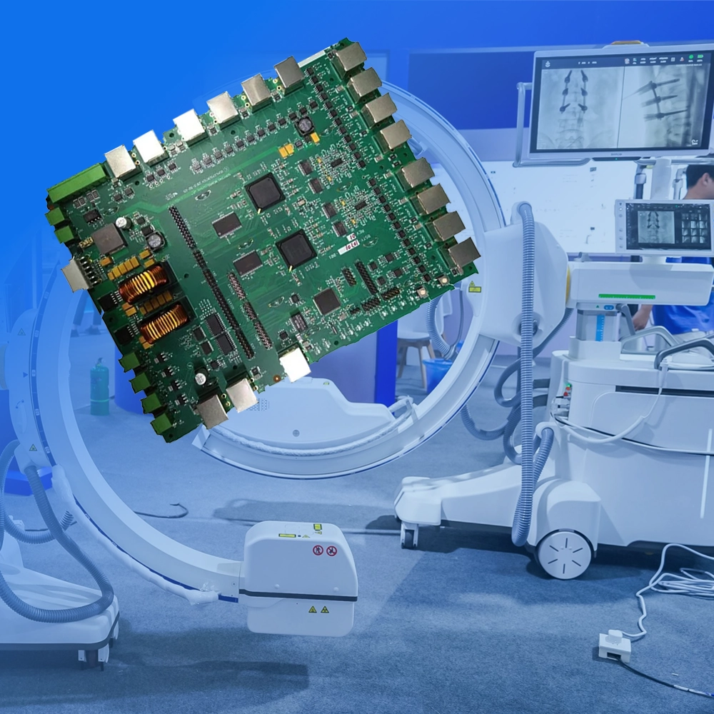
Why Protruding-Type Medical Imaging Probe PCBs Are RF Engineering Platforms
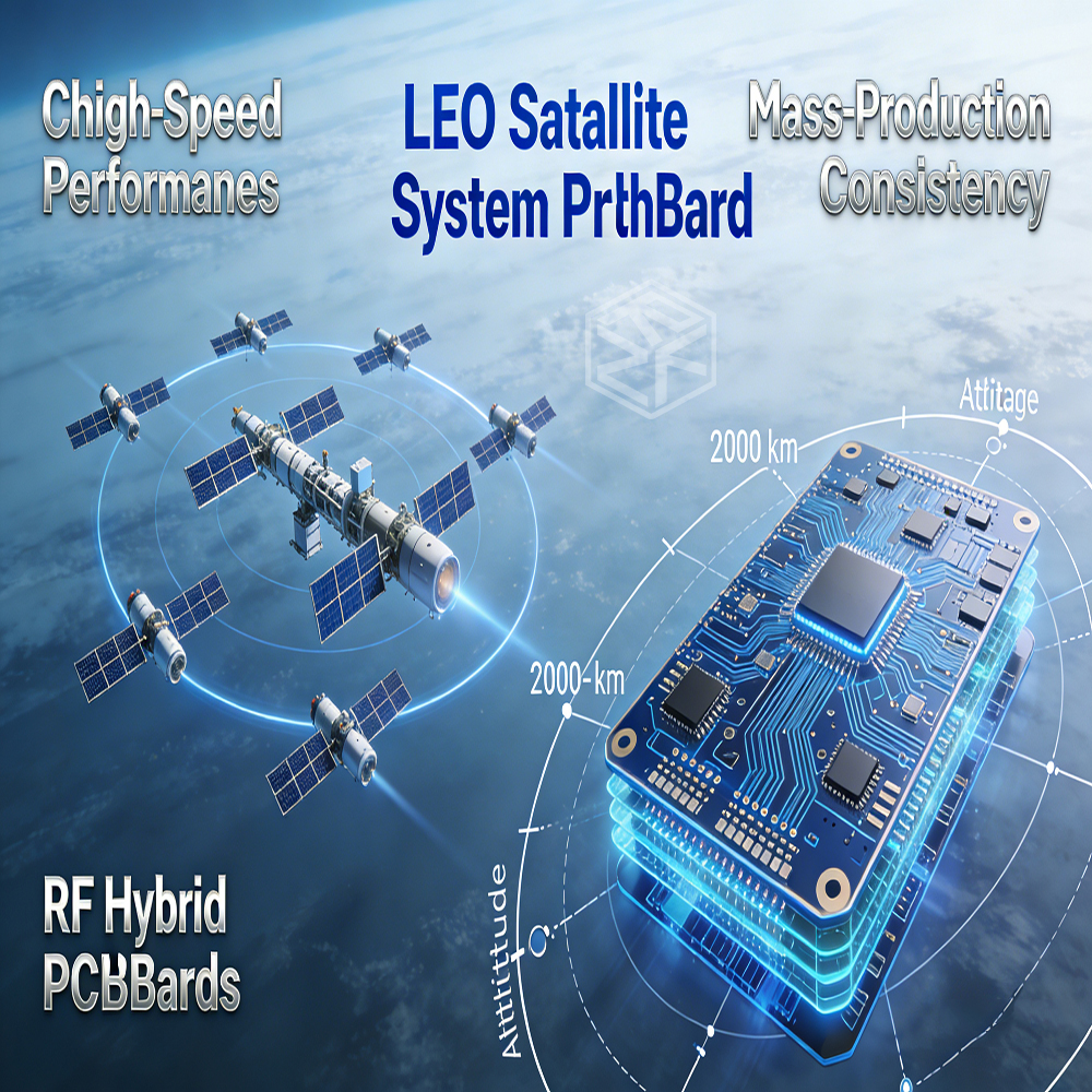
LEO Satellite PCB Requirements: High-Speed Performance & Mass Production Consistency

GEO Satellite PCB Design: Requirements for Ultra-Stable, High-Reliability Space Electronics
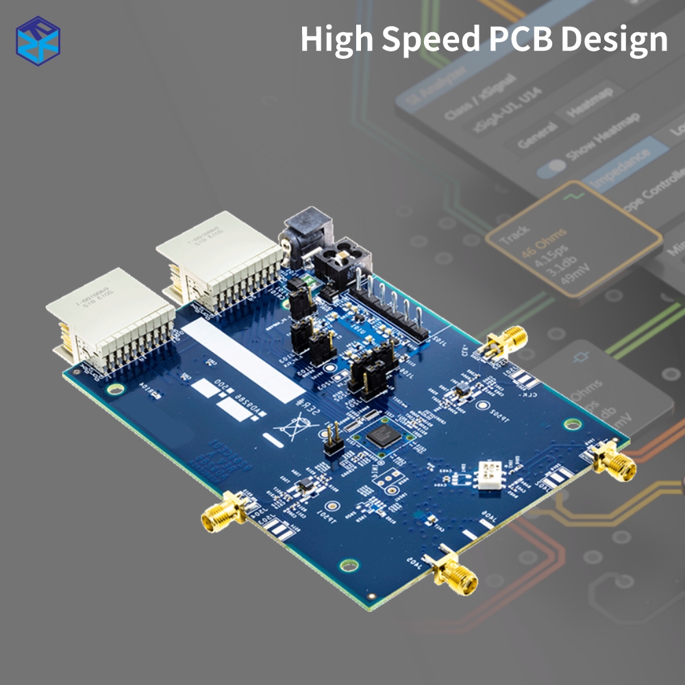
High-Speed PCB Design: Key Strategies for Enhanced Performance & Signal Integrity in Modern Electronics
High-Speed PCB Design. It covers core principles like Signal Integrity and Power Integrity, key technologies such as HDI, and advanced techniques for stack-up design and routing to maximize performance in modern electronics like AI servers and automotive systems. Learn how to overcome common challenges and ensure reliable, high-frequency operation.